
We do not yet have verified email-format data for
Labforinvention.
Visit the
Labforinvention company profile
for the full company information, employee directory, and
related contact signals. Email-format coverage is added as
new verified addresses are confirmed.
Explore related pages
Related company profiles:
Companies with email formats similar to Labforinvention


Free Chrome Extension
Find emails, phones & company data instantly
Find verified emails from LinkedIn profiles
Get direct phone numbers & mobile contacts
Access company data & employee information
Works directly on LinkedIn - no copy/paste needed
Aero Online
Your AI prospecting assistant
Select data to include:
Total price:
$0.00
0 records × $0.02 per record
How It Works
Get a Free Account
Sign up for a free account. No credit card required. Up to 10 free credits.

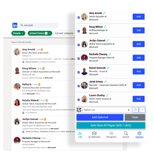
Search the #1 Contact Database
Get contact details of over 750M+ profiles across 60M companies – all with industry-leading accuracy. Sales Navigator and Recruiter users, try out our Email Finder Extension.
Use our AI-Powered Email Finder
Find business and personal emails and mobile phone numbers with exclusive coverage across niche job titles, industries, and more for unparalleled targeting. Also available via our Contact Data API.