
Csp Routing Business Development Lead
Currentleading SP routing business and consulting engineering in India market.
Dec 2021 - Present
Please complete the CAPTCHA to continue
@nokia.com
✓
LinkedIn matched
A concise factual answer block for searchers comparing this professional profile.
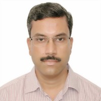
Anand Verma is listed as CSP routing business development lead at Nokia, a with 157111 employees, based in Delhi, India. AeroLeads shows a work email signal at nokia.com and a matched LinkedIn profile for Anand Verma.
Anand Verma previously worked as Regional Product Manager and consultant- APAC at Nokia and Regional Product Manager - India at Nokia. Anand Verma holds B. Tech, Electronics And Telcom from Knit Sultanpur, Up.
This section adds company-level context without repeating Anand Verma's masked contact details.
AeroLeads found 1 current-domain work email signal for Anand Verma. Compare company email patterns before reaching out.
B. Tech with 23+ years of experience:-Routing and SDN product and service specialist. - End to end design, engineering, operation, maintenance and testing of telecommunication network (access, backhaul and core, IP/MPLS/Segment routing and legacy), fixed broddband, Telco data center. - Business development for routing product and managed services, associated costing - WAN SDN: tech lead and BDM Specialties: JNCIS,
Listed skills include Ip, Mpls, Network Design, Broadband, and 16 others.
Company context helps verify the profile and gives searchers a useful next step.
A career timeline built from the work history available for this profile.
Gurugram, Haryana, India
leading SP routing business and consulting engineering in India market.
India
Regional PLM role for Routing, DC, SDN & IP-Optics joint solutions and consulting engineer for key accounts in APAC region.
India
Regional product line manager (PLM) role for both routing and SDN (NSP) for India region. This also includes assignments outside India and CXO level engagements.Draw account / customer level strategies across operators and market segments including Routing, BNG, SDN (NSP), Nuage, deepfield.
Gurgaon
E2E solution lead for Nokia routing portfolio for India market across all segments.doubling for business development lead for north India service provider market.
Gurgaon, India
Technical consultant for big service providers for IP/ MPLS and transport solutions including backbone, mobile/ multiplay backhaul and MPBN.responsible for creating both technical and commercial aspect of solution, also a single point of contact for customer for all technical issues in both pre-sales and post sales.
Gurgaon, India
- lead team of solution architect to deliver new service architecture from marketing requirement to operational readiness stage. - Single technical point of contact for any query on MS contract- managed services costing for new service launch
• Primary responsibility: draw reference network architecture for Bharti – Airtel’s telemedia wireline network and keep it updated for next 5 year. The base of this will be all IP network for all services: traditional voice (PSTN similation), triple play, application based services, etc.• Associated responsibility: assist solution architects to create solution specific to a service. Ensure that same is align to reference architecture.• Interact with team (business analysts, service roadmap analysts, solution architects) and customer to create reference network and framework to deliver the services.

• Worked as technical consultant for IP/MPLS and Metro/multiplay network to various service providers in India.• Represent Juniper in various forums as speaker.• Conducted partner and customer training on technology and products.• Conducted various PoC for Juniper routers and other devices.
lead information technology subgroup in TEC.written concept paper for NGN related topics for TEC's NGN compendium.advised DoT for various technical issues, related to license, regulation, etc.
Involve in design/ planning implementation and validation of IP network. Written specification for:• MPLS routers and CPE• Metro Area Network and metro Ethernet CPE• Content Delivery Network and Set Top box• NMS, OSS/ BSS• Data Centre Architecture and Enterprise Storage Infrastructure• ISP Traffic Legal Intercept and Monitoring System• DSLAM and DSL CPE, BRAS and NRAS; AAA, LDAP, etc.• Security devices: Firewall, IDS, IPSTesting for following• MPLS VPN network of BSNL• DSL based broadband network of BSNL• OSS/ BSS and Data Centre Architecture of BSNLOther activities• Design of BSNL’s Multiplay tender• Design and Evaluation of MTNL’s broadband tender• Design and Evaluation of MTNL’s Content Delivery Network tender• Design and Evaluation of BSNL’s SAN tender for CDR based billing• Study for IPv6, drafted the internal plan for the DoT for implementation of IPv6 in the country.• Study for NGN including IMS architecture, media gateway, signalling gateway, softswitch• Involved in formation of specification of WIMAX and broadband DLC network design for BSNL.

installation, operation and maintenace of telecom switching, routing and transmission network with associated facilities.This role was most demanding in terms of time as this involved:- installation: project management for timely installation of new telecom facilities from scratch, coordination with different function within the organisation (finance, civil, electrical, admin etc.), leading the installation team as a manager and as technical leader. - operation involves customer interface, fault repairing system management, addition/midification of subscriber for various services (telephone, internet, leased line, CDMA fixed wireless), interaction with higher and lower level nodes for seamless connectivity and also managing and leading the team.- maintenace includes troubleshooting any problem whether in equipment, outdoor (copper or fibre plant), connectivity with higher and lower level nodes, power plant, etc. End objective is to run show without breaks.- team management: for doing above activities, I had manged a team of 100+ people, spread across 3 revenue districts.
worked for telecom and SCADA projects for country's electric grid control. the requirement is to have a reliable telecom network (this includes fibre and microwave) and SCADA application running on it.
Other employees you can reach at nokia.com. View company contacts for 157111 employees →
 Qingxi Yuan
Colleague at NokiaBeijing, China
View →
SP
Qingxi Yuan
Colleague at NokiaBeijing, China
View →
SP
 Sumana Paul
Colleague at NokiaCroydon, England, United Kingdom
View →
AA
Sumana Paul
Colleague at NokiaCroydon, England, United Kingdom
View →
AA
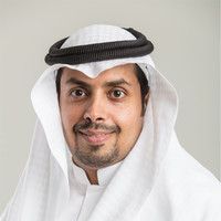 Abdullah Alsuaybi, Phd, Mba, Pmp®, Prince2®, Msp®, Csm®
Colleague at NokiaRiyadh, Saudi Arabia
View →
HR
Abdullah Alsuaybi, Phd, Mba, Pmp®, Prince2®, Msp®, Csm®
Colleague at NokiaRiyadh, Saudi Arabia
View →
HR
 Hari Rohit
Colleague at NokiaTumkur, Karnataka, India
View →
SK
Hari Rohit
Colleague at NokiaTumkur, Karnataka, India
View →
SK
 Siva Kalyan
Colleague at NokiaChennai, Tamil Nadu, India
View →
KM
Siva Kalyan
Colleague at NokiaChennai, Tamil Nadu, India
View →
KM
 Karolina Malanowska
Colleague at NokiaWroclaw Metropolitan Area, Poland
View →
YL
Karolina Malanowska
Colleague at NokiaWroclaw Metropolitan Area, Poland
View →
YL
 Yan Liang
Colleague at NokiaBeijing, China
View →
YF
Yan Liang
Colleague at NokiaBeijing, China
View →
YF
 Yuhanina Febri H.
Colleague at NokiaBanten, Indonesia
View →
DG
Yuhanina Febri H.
Colleague at NokiaBanten, Indonesia
View →
DG
 Diego Gimenez
Colleague at NokiaMiami-Fort Lauderdale Area, United States
View →
JW
Diego Gimenez
Colleague at NokiaMiami-Fort Lauderdale Area, United States
View →
JW
 Jason Wu
Colleague at NokiaHangzhou, Zhejiang, China
View →
Jason Wu
Colleague at NokiaHangzhou, Zhejiang, China
View →

Quick answers generated from the profile data available on this page.
Anand Verma works for Nokia.
Anand Verma is listed as CSP routing business development lead at Nokia.
AeroLeads has found 1 work email signal at @nokia.com for Anand Verma at Nokia.
Anand Verma is based in Delhi, India while working with Nokia.
Anand Verma has worked for Nokia, Alcatel-Lucent, Juniper Networks, Telecom Engineering Center, Dot, Govt Of India, and Bsnl.
Anand Verma's colleagues at Nokia include Qingxi Yuan, Sumana Paul, Abdullah Alsuaybi, Phd, Mba, Pmp®, Prince2®, Msp®, Csm®, Hari Rohit, and Siva Kalyan.
You can use AeroLeads to view verified contact signals for Anand Verma at Nokia, including work email, phone, and LinkedIn data when available.
Anand Verma holds B. Tech, Electronics And Telcom from Knit Sultanpur, Up.
Anand Verma is listed with skills including Ip, Mpls, Network Design, Broadband, Mpls Vpn, Network Architecture, Bgp, and Ospf.
Search by job title, company, industry, location, and seniority. Export verified B2B contact data when you need it.
Start free trial Search contactsCheck these profiles if this is not the Anand Verma you were looking for.