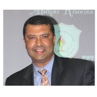
Ardy Sidhwa, Phd
AeroLeads people directory · profile

Ardy Sidhwa, Phd Email & Phone Number

Vice President of Operations at Pure Wafer
Location: Greater Phoenix Area, United States 6 work roles 3 schools
1 work email found @purewafer.com LinkedIn matched
✓ Verified August 2026 4 data sources Profile completeness 100%

Contact Signals · 1 work email

Work email a****@purewafer.com
LinkedIn Profile matched
3 free lookups remaining · No credit card
Current company
Role
Vice President of Operations
Location
Greater Phoenix Area, United States

Who is Ardy Sidhwa, Phd? Overview

A concise factual answer block for searchers comparing this professional profile.

Quick answer

Ardy Sidhwa, Phd is listed as Vice President of Operations at Pure Wafer, based in Greater Phoenix Area, United States. AeroLeads shows a work email signal at purewafer.com and a matched LinkedIn profile for Ardy Sidhwa, Phd.

Ardy Sidhwa, Phd previously worked as VP of Operations at Pure Wafer and Vice President of Manufacturing and Technology at Gv Semiconductor. Ardy Sidhwa, Phd holds Doctor Of Philosophy (Phd), Semiconductor Device Physics/ Electrical Engineering from University Of Arkansas.

Company email context

Email format at Pure Wafer

This section adds company-level context without repeating Ardy Sidhwa, Phd's masked contact details.

*@purewafer.com
68% confidence

AeroLeads found 1 current-domain work email signal for Ardy Sidhwa, Phd. Compare company email patterns before reaching out.

Profile bio

About Ardy Sidhwa, Phd

With over 27 years of groundbreaking contributions across Semiconductor Manufacturing, R&D, and Foundry Operations, I have established a solid foundation in process integration, device yield enhancement, and advanced semiconductor technologies. My expertise spans nanotechnology, materials characterization, sustainability, and the design and development of solar cells. I deeply understand semiconductor manufacturing methods, wafer surface cleaning techniques, nanoparticle reduction, and advanced parts cleaning.As an executive, I’ve managed technology product portfolios through global semiconductor foundries, applied lean manufacturing principles, and implemented cutting-edge quality assurance systems. My innovations have resulted in multiple patents and publications, supported by a robust business acumen and a proven ability to drive operational excellence.I am passionate about hard work and maintaining a strong customer focus. I have demonstrated success in turning around underperforming teams, facilities, and operations. My leadership approach is centered on building scalable, uniform business models while fostering high-integrity leaders who deliver measurable improvements in sales, operations, and service.A results-driven professional, I’ve successfully developed technology strategies for alliances and joint ventures, consistently meeting business goals and customer needs.Career Highlights:• Vice President of Operations Worldwide, Pure Wafer Inc.• Vice President of Manufacturing and Technology, GV Semiconductor• Senior Director, Innovation and Technology, Quantum Global Technologies, LLC• Senior Site Staff, ATMEL Semiconductor• Chief Operating Officer (COO) & Senior Executive Board Member, Armor Designs, Inc.• Director of Corporate Process Technology & Quality Director, STMicroelectronics Inc.• Executive Board Member, Green Power Resource Management, Inc. (GPRM)With 7 U.S. patents and over 100 interdisciplinary publications, I am highly motivated to embrace new challenges and consistently deliver value to my clients and partners.

Listed skills include Semiconductors, Failure Analysis, Manufacturing, Ic, and 46 others.
Current workplace

Ardy Sidhwa, Phd's current company

Company context helps verify the profile and gives searchers a useful next step.

Pure Wafer
Pure Wafer
Vice President of Operations
AeroLeads page
6 roles

Ardy Sidhwa, Phd work experience

A career timeline built from the work history available for this profile.

Vp Of Operations

Current

San Jose, California, Us

• Manage Arizona (Prescott) and California (San Jose) operations and new product development.• In association with the Chief Executive Officer, direct the corporate development activities of the Company, subsidiaries, and associated companies. Ensured proposals for key new licensing arrangements, mergers, acquisitions, divestments, and closures. Evaluate significant operational developments prior to Board presentation for approval.• Inform the CEO on all matters that may be of importance to the Group, including its current performance and processes.• Responsible for appointing senior directors and managers for the organization of the Company.• Responsible for managing operations and exercising executive stewardship of the Company's physical, financial, and human resources.• Facilitate and direct programs and solving issues related to wafer surface cleaning processing, logistics, yield, and failure analysis for current and new technologies.

Jun 2019 - Present

Vice President Of Manufacturing And Technology

Gv Semiconductor

* Goal of our company is to enable advanced power conversion with innovative power semiconductors and system design. * Responsible for the setup of manufacturing fab and development of process technology for GVS worldwide. * Direct and interact with other GVS sites, external foundries, vendors and suppliers and assessed their process technology, capability and product reliability for submicron technologies.* Facilitate defined programs and solved issues related to processing, logistics, and yield and failure analysis for a new technology chip test vehicle for key GVS products.* Assist in the design, layout, and manufacturing of Power devices using GaN structures

Apr 2017 - Jul 2019

Sr. Director, Innovation And Technology (R&D)

Quantum Global Technologies, Llc (Quantumclean)

* Develop and manage Advanced Technology Cleaning Centers (ATCC) for Quantum Global Technologies (QuantumClean & ChemTrace) globally* Engage Quantum Global Technologies (QuantumClean & ChemTrace) R&D team with Sematech research team for collaborative work on Nanoparticles in solution* Develop Advanced Cleaning, Coating, and Analytical Methods for sub 14nm technology nodes to support current and future 2D and 3D Integrated Circuits* Manage and develop a group of R&D scientists to lead in Novel Surface Cleaning processes, understanding of defect and process integration for semiconductor chip manufacturers, and Nanoparticle Control in solution and on different substrates * Responsible for the Fundamentals of Novel Surface Cleaning, Advance Cleaning Techniques, Nanoparticle Detection in Solution, and Nanoparticle Control in Solution* Characterization of current optical liquid particle counters, as well as evaluation of alternative sizing and counting techniques* Develop best known methods for counting and determining particle size* Characterization and benchmarking of chemical filters from major suppliers for sub-10 nm particle filtration* Understanding of new methods to determine dissolved solids in UPW and chemicals* Development of new methods to identify sources of particle shedding and chemical leaching by different components used for cleaning applications * Computational modeling of particle and surface interactions * Understanding of liquid purification based on acoustic, optical and electrical techniques

Dec 2013 - Apr 2017

Sr. Staff Manager

San Jose, Ca, Us

• Managing Manufacturing Operations, Process Integration, and Product Yield Enhancement for state of the art Microcontrollers and Memory products • Ability to influence, mentor and lead multi functional organizations including Process and Equipment Engineering, Manufacturing, and Facilities to achieve world class products. • Interface with Quality group to ensure that customer return feedback results are focused and appropriate corrective actions in the manufacturing line are taken to insure continuous quality improvements. • Build and maintain a positive, high performance culture that produces top results with continuous improvement and world class products.• Drive manufacturing wide defectivity improvement program and develop the zero defect culture across the company.

Aug 2011 - Dec 2013

Chief Operating Officer And Sr. Executive Board Director

Armor Designs, Inc.

• Managed worldwide Operations and New Product Development • Facilitated and directed programs and solving issues related to armor processing, logistics, yield and failure analysis for a new technology• Assisting in the design, layout, and manufacturing of composite armor materials and development of new materials to accommodate various threat levels• Responsible for managing the business, exercising executive stewardship of the Company’s physical, financial and human resources.• Appointed senior directors and managers for the organization of the Company.• Achieved ISO 9001:2000 certification of registration for the Manufacturing of Composite Body Armor for Armor Designs, Inc. within six months of initiating the process.• In association with the Executive Chairman, involved in directing the corporate development activities of the Company, Subsidiaries and Associated Companies and ensuring proposals for major new licensing arrangements, mergers, acquisitions, divestments, closures and significant operational developments are properly evaluated, prior to their presentation to the Board for approval.• Ensuring that appropriate policies and strategies are adopted within the Company that these policies and strategies are implemented effectively, that performance is effectively monitored and that guidance or direction is given where appropriate.• Informed the Executive Chairman on all matters that may be of importance to the Group, including its current performance and processes.

Nov 2007 - May 2011

Corporate Process Technology / Quality Manager

Geneva, Switzerland, Ch

While ST transitioned towards a leaner manufacturing model, much emphasis was placed on interactions with other ST R&D and manufacturing facilities, and manufacturing tool vendors. Quality, Cost, and On-time Deliveries to our customers were key priorities. •Implemented Quality programs and functions for Phoenix operations •Directed the overall manufacturing expansion from 4400 Wafers per week to ~7000 Wafers per week•Senior Director, Corporate Process Technology Department. Had direct interaction with other ST sites, foundries, and external vendors, on assessing their process technology, capability and product reliability below 130nm and 90nm technologies. • Facilitated multiple programs related to manufacturing processing, yield, and failure analysis for a new chip test vehicle among all ST sites.• Assisted in the design, layout, and manufacturing of metal interconnect structures to accommodate complex circuitry for different ST facilities. • Responsible for the evaluation of metallurgical and mechanical properties of metal interconnects and thin film properties used for advanced IC’s.• Transferred critical technical knowledge to different manufacturing sites in limited time.• Exceeded the target of $5M per manufacturing facility due to the implementation of novel processing methods.• Solved all IC process related technical problems for Back-End of the Line (BEOL) for all 8-inch and 6-inch facilities around the world (Asia, Europe, and USA). • Deployed new process innovation and new design concepts to achieve optimum manufacturing capability among all ST fabrication sites.• Coordinated quarterly technical reviews and user meetings with different manufacturing tool suppliers like AMAT, Novellus, ASM, LAM etc., for Continuous Improvement Projects (CIP), tool performance, and new product deployment. • Lead and directed the Process Technical Committees (PTC) managers towards best manufacturing excellence by deploying lessons learned among all ST sites.

Oct 1995 - Jan 2008
3 education records

Ardy Sidhwa, Phd education

Doctor Of Philosophy (Phd), Semiconductor Device Physics/ Electrical Engineering

University Of Arkansas

Master Of Science (Msc), Electrical And Electronics Engineering

University Of Arkansas

Bachelor Of Science (Bsc), Electrical And Electronics Engineering

University Of Arkansas
FAQ

Frequently asked questions about Ardy Sidhwa, Phd

Quick answers generated from the profile data available on this page.

What company does Ardy Sidhwa, Phd work for?

Ardy Sidhwa, Phd works for Pure Wafer.

What is Ardy Sidhwa, Phd's role at Pure Wafer?

Ardy Sidhwa, Phd is listed as Vice President of Operations at Pure Wafer.

What is Ardy Sidhwa, Phd's email address?

AeroLeads has found 1 work email signal at @purewafer.com for Ardy Sidhwa, Phd at Pure Wafer.

Where is Ardy Sidhwa, Phd based?

Ardy Sidhwa, Phd is based in Greater Phoenix Area, United States while working with Pure Wafer.

What companies has Ardy Sidhwa, Phd worked for?

Ardy Sidhwa, Phd has worked for Pure Wafer, Gv Semiconductor, Quantum Global Technologies, Llc (Quantumclean), Atmel Corporation, and Armor Designs, Inc..

How can I contact Ardy Sidhwa, Phd?

You can use AeroLeads to view verified contact signals for Ardy Sidhwa, Phd at Pure Wafer, including work email, phone, and LinkedIn data when available.

What schools did Ardy Sidhwa, Phd attend?

Ardy Sidhwa, Phd holds Doctor Of Philosophy (Phd), Semiconductor Device Physics/ Electrical Engineering from University Of Arkansas.

What skills is Ardy Sidhwa, Phd known for?

Ardy Sidhwa, Phd is listed with skills including Semiconductors, Failure Analysis, Manufacturing, Ic, Semiconductor Industry, Silicon, Electronics, and R&D.

Find 750M verified contacts

Search by job title, company, industry, location, and seniority. Export verified B2B contact data when you need it.