Director, Adv. Moudle Development And Td
Sien(Qingdao) Intergrated Circuits Co.,Ltd.
Please complete the CAPTCHA to continue
@163.com
✓
LinkedIn matched
A concise factual answer block for searchers comparing this professional profile.
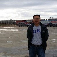
Ben Yang is listed as Director, Adv. Moudle Development and TD at SiEn(QingDao) Intergrated Circuits Co.,Ltd., based in Inner Mongolia, China. AeroLeads shows a work email signal at 163.com and a matched LinkedIn profile for Ben Yang.
Ben Yang previously worked as Director, Adv. Moudle Development/TD at Sien(Qingdao) Intergrated Circuits Co.,Ltd. and 副所长 at 国电投中央研究院. Ben Yang holds Doctor Of Philosophy (Phd), Materials Science from Shanghai Jiao Tong University.
This section adds company-level context without repeating Ben Yang's masked contact details.
AeroLeads found 1 current-domain work email signal for Ben Yang. Compare company email patterns before reaching out.
13 yrs R&D,Operation & Management, Startup, Business and P&R experience in semiconductor and solar industry. Strong people management and performance management skill with more than 10 yrs managing experience. Strong leadership and great team player. Excellent communication and negotiation skills, be good at push vendors to provide effective technical and supply chain support, based on double win. Strong project management experience and capability, based on result orientation Well known QE,good knowledge and experience of SPC,CIT and Cost down. Experience and skill in P&R, financing and business, based on customer satisfaction. Knowledge of finance. Key contribution to SMIC 65nm and 45nm Logic process R&D. Strong process and hardware knowledge of PVD, CVD and ECP. Strong trouble shooting skill, especially of finding root cause of hardware issue by DOE. Integration knowledge of Logic and Dram process. Well known hetero-junction Solar cell process. Limited knowledge of other modules, such as Wet, CMP, RTP, Furnace and ETCH Ph. D degree in Shanghai Jiaotong University, majored in material science. Over 40 patents and 10 papers
Listed skills include Semiconductors, Ic, Semiconductor Industry, Process Integration, and 19 others.
Company context helps verify the profile and gives searchers a useful next step.
A career timeline built from the work history available for this profile.
Inner Mongolia, China
Qingdao
中国 北京市区
Huhehaote
Responsible for 1.5 GW cell/module start-up and operation, EPC business, including technology and equipment evaluation and business negotiation, facility construction, Fab operation, team built-up, QE, supply chain, sales, OEM, PR,ESH,IT, financing and EPC business development. Facility over 400000 m2 built, EQ purchasing negotiation completed, a 200MW EPC contract signed, located on East-China
Hangzhou, Zhejiang, China
Function on process transfer and development, Module OEM management, Fab QE& ESH, PR and financing, Automation development, Fab startup. Cell technology transfer and development from US pilot line to China production line, yield improved from 30% to 95% with Avg. efficient of 20.9% by improve process, optimize hardware and control Fab mini-environment. Module technology development Module OEM management: OEM plant evaluation, pilot run ,reliability qualification, business negotiation, module production and quality control, cost down, supply chain management. . Fab automation development and bussiness negotiation. Build up Fab Q&E, supervise ESH Function on P&R, built up good relationship with both China and Zhejiang Government Energy Bureau.Promoted Silevo to win National energy area science project recognition of, host by China Energy Bureau. Silevo was the only joint venture to get the reward. Reported PV status and made suggestion to Development research center of the State Council of PRC Working on financing for Fab capacity expansion, negotiation with investors..
Nantong, Jiangsu, China
Responsible for new process & tool evaluation, in-charge of operation of pilot line, manage over 50 engineers and operators. Rebuilt and manage pilot line with 5S.

Shanghai City, China
Responsible for TF Dept. for metal and dielectric film deposition developing for 55nm, 45/40nm and 32/28 logic process (300 mm), directly managed 3 senior managers with 3 teams at SH and BJ sites. supervised all TD modules at BJ, partially. 32 nm process study and tool evaluation. Fixed INWE of 40nm by optimizing SMT (Stress memory technology), shorting developing cycle 6 months. Top3 department of innovation (patents application and authorization) since 2007. All the 3 three teams within top 10 in 2010.
Beijing City, China
Responsible for Metallization Dept. and DCVD Dept. for metal and dielectric film deposition developing for 45nm, 40nm and beyond logic process (300 mm), including PVD, MOCVD, ECP, HDP, SACVD, PECVD and HARP Metal group is the most stable and efficient team among all modules. Stabilize DCVD team by encouraging engineer on meeting and one to one talking. Fixed 45nm NiSix piping issue by a novel concept, improved yield from 5% to 45% and more cost effective than IBM process. Improved NiSix RS to meet target by optimizing RTA and Ni-Pt deposition. Found root cause and solution of 45nm EM fail. Fixed one SACVD chamber heaters mismatch issue within one month, which had been over half an years by disciplining vendor and discussing detail with them on site. Developing void free PMD HARP process for 45nm and 40nm.
Shanghai City, China
Responsible for process maintain, trouble shooting, defect reduction and engineer management of a group within PVD section, including the process of STD Co, Ti and AL PVD, IMPTi, SIPTi, MOCVD, TiCl4 and Wsix (200 mm), leading 8 engineers. Responsible for SPC and OCAP review of metal section and report to dept. manager weekly. Co-work with PIE and TD for 0.25, 0.18, 0.09um Logic and 0.20,0.18, 0.11um DRAM process developing and trouble shooting. Found root cause of one Al defect, and coordinated QE, PIE, Facility to fix the issue by separating CMP area with other area both on Fab and sub-Fab. The way was followed by other 3 Fabs.
Wsix(TEL), Co PVD(AMAT) tool set up, process qualification, trouble shooting and process maintain. Finished one CIT project, improved WSix WPH 20%. Fixed Co deposition tool yield low issue and improved yield 1.5%.

Quick answers generated from the profile data available on this page.
Ben Yang works for SiEn(QingDao) Intergrated Circuits Co.,Ltd..
Ben Yang is listed as Director, Adv. Moudle Development and TD at SiEn(QingDao) Intergrated Circuits Co.,Ltd..
AeroLeads has found 1 work email signal at @163.com for Ben Yang at SiEn(QingDao) Intergrated Circuits Co.,Ltd..
Ben Yang is based in Inner Mongolia, China while working with SiEn(QingDao) Intergrated Circuits Co.,Ltd..
Ben Yang has worked for Sien(Qingdao) Intergrated Circuits Co.,Ltd., 国电投中央研究院, Inner Mongolia Clean Air Electronic Materials Inc., Silevo China, and Hanwha Solarone.
You can use AeroLeads to view verified contact signals for Ben Yang at SiEn(QingDao) Intergrated Circuits Co.,Ltd., including work email, phone, and LinkedIn data when available.
Ben Yang holds Doctor Of Philosophy (Phd), Materials Science from Shanghai Jiao Tong University.
Ben Yang is listed with skills including Semiconductors, Ic, Semiconductor Industry, Process Integration, Cmos, Silicon, Product Engineering, and Failure Analysis.
Search by job title, company, industry, location, and seniority. Export verified B2B contact data when you need it.
Start free trial Search contactsCheck these profiles if this is not the Ben Yang you were looking for.
View similar profiles