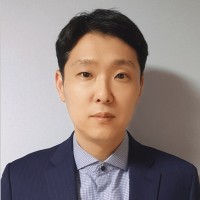
AeroLeads people directory · profile

Bk Kwon Email & Phone Number

Sr Member of Technical Staf at S semiconductor at S semiconductor
Location: Pahang, Malaysia 2 work roles 2 schools
LinkedIn matched
✓ Verified August 2026 3 data sources Profile completeness 86%

Contact Signals

LinkedIn Profile matched
3 free lookups remaining · No credit card
Current company
S semiconductor
Role
Sr Member of Technical Staf at S semiconductor
Location
Pahang, Malaysia

Who is Bk Kwon? Overview

A concise factual answer block for searchers comparing this professional profile.

Quick answer

Bk Kwon is listed as Sr Member of Technical Staf at S semiconductor at S semiconductor, based in Pahang, Malaysia. AeroLeads shows a matched LinkedIn profile for Bk Kwon.

Bk Kwon previously worked as Sr Member of Technical Staff at S Semiconductor and Staff Engineer at M Semiconductor. Bk Kwon holds Bachelor'S Degree, Electrical And Electronics Engineering, 3.8/4.0 from Chungbook National Univisity.

Profile bio

About Bk Kwon

* Process Integration and Device engineering as a Senior Member of Technical Staff18+ years work experiences of process integration, device, products development & foundry business 10 years overseas working experience with good communication and management skills in multinational company, in charge of developing high voltage devices, power discrete devices, and its process integration, etc. 8 years engineering working experience in various process and products developments, such as 18volts & 32volts & 100volts high voltage process/products for small DDI & large DDI applications. Successful project management experience with excellent teamwork. Good technical background supporting, well experienced in customer communication, problem solving, data analyzing and an excellent ability to lead and communicates with other teams & customers.  Familiar with process integration, process/quality control, and continual improvement methods, with experienced in 6 Sigma, SPC, JMP, Minitab, CP/CPK, FMEA and 8D report, good analytical and trouble-shooting skills, including handling of manual testers (Agilent4156, Keithley & CV analyzer). Well experienced with layout tools and mask making works for test vehicle generation including test pattern design and layout with Cadence opus tool & Layed tool.

Current workplace

Bk Kwon's current company

Company context helps verify the profile and gives searchers a useful next step.

S semiconductor
S Semiconductor
Sr Member of Technical Staf at S semiconductor
2 roles

Bk Kwon work experience

A career timeline built from the work history available for this profile.

Sr Member Of Technical Staff

Current
S Semiconductor

Malaysia

* Process Integration and Device engineering as a Senior Member of Technical Staff• In charge of developing Power Discrete Device & Process, such as Split-Gate-Trench-MOS process with Deep Trench and Dual Poly for 40V to 100V applications. - 3 devices under development for 40V to 100V applications with China & USA customers• Successfully developed high voltage process based on 0.18um & 0.20um STI (Shallow Trench Isolation) & DTI (Deep Trench Isolation) process for Large-panel Driver-IC such as 18volt & 13.5volt & 9volt applications.- Developed 2.0um 18volt HV process with STI base for LDDI application- Developed 0.18um 18volt/ 13.5volt/ 9volt HV process with STI base for LDDI application- Developed 0.18um 18volt HV process with DTI base for LDDI application• In charge of technology transfer from other fab for 0.18um & 0.25um 18volts process and products, and successful yield demonstration.- Successfully transferred the 0.18um & 0.25um 18volt technology from other fab (in Taiwan), including mask generation, process flow integration with modified conditions, electrical analysis & matching, physical analysis, yield demonstration, and product qualification for mass production• Contributed and involved in High voltage technology transfer to other foundry fabs, such as 0.18um 32volts process & products- Transferred 0.18um 32volt process to Malaysia fab, and mass production- Transferred 0.18um 32volt process to China fab• Performed product development for small-DDI applications, such as 32volts & 21volts process with 0.15um & 0.18um STI logic process, production yielding upto 98%.- Developed various sDDI products for China & Taiwan customers and mass production• Developed mask reduction process for 0.13um & 0.18um 32volt process- Process integration, creating new mask generation rule, and electrical analysis for performance matching and comparable yielding in production

Jan 2008 - Present

Staff Engineer

M Semiconductor

Korea

* Process Integration and Product development as a Staff Engineer• Until 2008, developed 0.15um 30volts high voltage process with 2.24um2 SRAM, and Isolated HV-MOS process. - In charge of 0.15um 30volts high voltage products development for TFT LDI and OLED applications- In charge of 0.22um 18volts high voltage products development for Large DDI applications• Until 2007, developed 0.15um 30volts high voltage process with 3.27um2 SRAM. - In charge of 0.18um 30volts high voltage products development for TFT LDI- In charge of 0.35um 18volts high voltage products development for Large DDI- In charge of 0.6um high voltage products development (25volts, 40volts, and 80volts) for TFT LDI, Source & Gate driver applications• Until 2005, in charge of 0.18um/ 2.0um high voltage products development.- Developed 1.4um 150volt high voltage process with SOI wafer materials

Dec 2000 - Jan 2008
2 education records

Bk Kwon education

Bachelor'S Degree, Electrical And Electronics Engineering, 3.8/4.0

Chungbook National Univisity
FAQ

Frequently asked questions about Bk Kwon

Quick answers generated from the profile data available on this page.

What company does Bk Kwon work for?

Bk Kwon works for S semiconductor.

What is Bk Kwon's role at S semiconductor?

Bk Kwon is listed as Sr Member of Technical Staf at S semiconductor at S semiconductor.

Where is Bk Kwon based?

Bk Kwon is based in Pahang, Malaysia while working with S semiconductor.

What companies has Bk Kwon worked for?

Bk Kwon has worked for S Semiconductor and M Semiconductor.

How can I contact Bk Kwon?

You can use AeroLeads to view verified contact signals for Bk Kwon at S semiconductor, including work email, phone, and LinkedIn data when available.

What schools did Bk Kwon attend?

Bk Kwon holds Bachelor'S Degree, Electrical And Electronics Engineering, 3.8/4.0 from Chungbook National Univisity.

Find 750M verified contacts

Search by job title, company, industry, location, and seniority. Export verified B2B contact data when you need it.

People with similar names

Check these profiles if this is not the Bk Kwon you were looking for.

View similar profiles