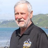

AeroLeads people directory · profile
Daryl New Email & Phone Number
President
at
Quantum Innovation & Execution
LinkedIn matched
✓ Verified July 2026
3 data sources
Profile completeness 86%
Who is Daryl New? Overview
A concise factual answer block for searchers comparing this professional profile.
Quick answer
Daryl New is listed as President at Quantum Innovation & Execution, based in Boise, Idaho, United States. AeroLeads shows a matched LinkedIn profile for Daryl New.
Daryl New previously worked as Founding President at Boise Medtronics and Sr Program Manager at Micron Technology. Daryl New holds Master Of Business Administration - Mba, Business Statistics from University Of Phoenix.
Company email context
Email format at Quantum Innovation & Execution
This section adds company-level context without repeating Daryl New's masked contact details.
Quantum Innovation & Execution
Review company-level records connected to Daryl New before choosing the right outreach path.
Profile bio
About Daryl New
Strong influencer with proven results. Driven to innovate and execute extremely complex technical programs through success. Metrics and Statistics driven, with a keen eye for overlooked details, mitigating and removing risks. Relied upon in critical situations to drive direction in achieving targets and goals. Advanced level of troubleshooting skills necessary in today's interaction affect driven environment.
Current workplace
Daryl New's current company
Company context helps verify the profile and gives searchers a useful next step.
12 roles · 44 years
Daryl New work experience
A career timeline built from the work history available for this profile.
President
CurrentApplying FMEA and Strategic Direction Consulting in 5G, Edge Computing, AI, Neural Networks, Emerging Technology, Systems Engineering, Semiconductors.
2017 - Present
~9 yrs 6 mos

Founding President
CurrentElectronic Muscle Stimulators. Best in class device physics model application.
2018 - Present
~8 yrs 6 mos

Sr Program Manager
Plan, coordinate and influence best in class semiconductor memory new product introduction. Work closely with design, process R&D, device modeling and production to launch timely high value quality memory products.LPDDR4 20nm qualification was off target and risking the company 30% (~ $6 Billion Dollars) of total expected revenue. Brought in to quickly hire and assemble a team of subject matter experts to determine root cause and tier 1 customer qualify the entire program. Identified root cause with team members using an advanced skill set of physical, electrical, and statistical analysis.Determined and removed root cause failure from the system enabling LPDDR4 20nm product to qualify as Tier 1 and become the highest quality part with the highest demand in the industry. Revenue increased to over $7 Billion per quarter.
2014 - 2016
~2 yrs
R&D Dram Npi Program Manager
Called upon as an All Hands on Deck influencer to help solve extremely complex problems within the semiconductor community.
2000 - 2003
~3 yrs
Yield Enhancement Engineer
Member: Electronic Device Failure Analysis Society and International Symposium for Testing and Failure Analysis.Spearhead product yield improvement activities through electrical failure analysis (EFA), data analysis and knowledge of product design and operation;Organize working group that is responsible in understanding yield issues, identifying root cause of failure and designing and implementing fixes;Understand all electrical testing done at Probe test;Perform electrical characterization on the bench tester for the failing device and create failure model based on the data collected;Understand Fab process and physical failure analysis (PFA) methodologies to be able to come up with physical defect models that explain the failure;Work closely with Yield Engineers and Process Integration Engineers to help them quickly determine where to look for physical defects and confirm defect pictures match electrical signatureWork with other engineering teams to resolve testing issuesSupport and develop new tools and techniques to localize and identify device failuresRecognize, identify, and raise awareness of process issues to appropriate teamsAttend necessary meetings and present results to process and integration teamsPossibly travel to manufacturing sites during transfer of next-generation processes, using the latest data analysis techniques and methods
1999 - 2001
~2 yrs
Parametric Lead Design Engineer
Strong background in solid state physics, semiconductor processing and device characterizationStrong understanding of device operation in memory systems including NAND, DRAM, PCM, storage class, and cross-point memoriesAbility to independently learn new memory systemsStrong data analysis skills and experience in automating data analysis methodsExperience in the operation and automation of semiconductor instrumentation including, but not limited to:Parameter analyzers, SPA, SMULCR metersNetwork analyzersOscilloscopesPulse & waveform generatorsWafer probersATE and bench systemsKnowledgeable in a variety of software tools and operating systems, including but not limited to: Python/Pandas/PyQtC/C++Unix/LinuxPerlSQLJMP/JSL
1997 - 1999
~2 yrs
Ferroelectric R&D Process Development
Analyze and report experimental correlations, interaction and first order effectsAntifuse Circuit Worldwide Program ManagerYield Development/EnhancementFerroelectric R&D process developmentPhotolithography process developmentPlasma Vapor Deposition developmentReactive Ion Etching developmentIon Etching development
1994 - 1997
~3 yrs
Photo-Lithography
Micron Technology
Micron initiated a strong cost reducing program. Lead small team in photo resist reduction and critical dimension variation reduction. Tier 1 qualed a dynamic resist dispense while reducing variation 20%. Reducing consumables and variation saved the company over $3 Million per year.responsible for sustaining and making the improvement efforts to yield and equipment performance in your process area, to achieve high device yield, reliability, and cost efficiency. You have to establish processes, set up parameters, and carry out evaluation to improve process and equipment performances.1.Establish and improve process condition and technology.2.Upgrade process capability and reduce production cost.3.Establish and modify process management projects.4.Set up process parameters of equipment.5.Evaluation, promotion and planning of new equipment / materials.6.Abnormal analysis and improvement.
1991 - 1994
~3 yrs
Photolithography
A commitment to work in a safe manner and contribute to a safe working environment.3+ years Photo track equipment experience required.Thorough understanding of photo track hardware and software.Ability to make new Photo track recipes and wafer flows.Strong communication skills in written, verbal, and presentation formats.Understand each photo process step and its impact on photo performance.Use photo track knowledge to troubleshoot process issues.The ability to use schematic diagrams to troubleshoot systems.A strong mechanical aptitude with the ability to understand and troubleshoot mechanical systems.Demonstrate analytical problem solving and equipment troubleshooting skills.Time-management, multitasking, and priority setting skills.Proficiency in MS Office tools and Micron wafer and chemical tracking systems.A high level of self-motivation.Able to follow directions on complex projects.Interface with equipment vendors and facilities members in a professional manner.Ability to work independently or in a team environment.Good organization and documentation skills.Proven ability in multi-tasking complex projects and enjoy working in a fast pace environment.Display of Micron behaviors, with minimal supervision.
1988 - 1991
~3 yrs

Avionics
1988 - 1991
~3 yrs

Tactical Communications & Intel
Advanced Encrypted Communications and Defense SystemsSecret Security ClearanceFort Dix, NJFort Sill, OK*Classified*
1983 - 1991
~8 yrs
3 education records
Daryl New education

Master Of Business Administration - Mba, Business Statistics

Bachelor'S Degree, Marketing/Marketing Management

Bachelor Of Applied Science - Basc, Electrical And Electronics Engineering
FAQ
Frequently asked questions about Daryl New
Quick answers generated from the profile data available on this page.
What company does Daryl New work for?
Daryl New works for Quantum Innovation & Execution.
What is Daryl New's role at Quantum Innovation & Execution?
Daryl New is listed as President at Quantum Innovation & Execution.
Where is Daryl New based?
Daryl New is based in Boise, Idaho, United States while working with Quantum Innovation & Execution.
What companies has Daryl New worked for?
Daryl New has worked for Quantum Innovation & Execution, Boise Medtronics, Micron Technology, Boise Airport - Boi, and Us Army.
How can I contact Daryl New?
You can use AeroLeads to view verified contact signals for Daryl New at Quantum Innovation & Execution, including work email, phone, and LinkedIn data when available.
What schools did Daryl New attend?
Daryl New holds Master Of Business Administration - Mba, Business Statistics from University Of Phoenix.
Find 750M verified contacts
Search by job title, company, industry, location, and seniority. Export verified B2B contact data when you need it.
Start free trialPeople with similar names
Check these profiles if this is not the Daryl New you were looking for.
View similar profiles