
AeroLeads people directory · profile
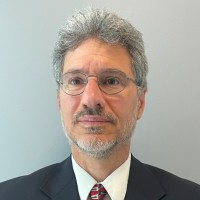
David Brunco Email & Phone Number
Principal IP Technologist, Memory and Processor Devices
at
Wheatstone IP Law Corporation
1 work email found
@alum.mit.edu
1 phone found area 408
LinkedIn matched
✓ Verified Jul 2026
4 data sources
Profile completeness 100%
Current company
Role
Principal IP Technologist, Memory and Processor Devices
Location
Greater Pittsburgh Region, United States
Company size
Who is David Brunco? Overview
A concise factual answer block for searchers comparing this professional profile.
Quick answer
David Brunco is listed as Principal IP Technologist, Memory and Processor Devices at Wheatstone IP Law Corporation, a with 5 employees, based in Greater Pittsburgh Region, United States. AeroLeads shows a work email signal at alum.mit.edu, phone signal with area code 408, and a matched LinkedIn profile for David Brunco.
David Brunco previously worked as Principal IP Technologist, Memory & Processor Devices at Wheatstone Ip Law Corporation and Patent Analyst at Semipat Consulting. David Brunco holds Phd, Materials Science And Engineering, Gpa 3.9/4.0 from Cornell University.
Company email context
Email format at Wheatstone IP Law Corporation
This section adds company-level context without repeating David Brunco's masked contact details.
{first_initial}{last}@alum.mit.edu
86% confidence
AeroLeads found 1 current-domain work email signal for David Brunco. Compare company email patterns before reaching out.
Profile bio
About David Brunco
Primary expertise in semiconductor process integration, process engineering and patents, but also hands-on contributor to device, yield, waste reduction, and quality control. Demonstrates strong project management and team leadership. Works across different business groups to solve problems. Awarded 30 US patents.
Listed skills include Nanotechnology, Spc, Ic, R&D, and 50 others.
Current workplace
David Brunco's current company
Company context helps verify the profile and gives searchers a useful next step.
Wheatstone Ip Law Corporation
12 roles
David Brunco work experience
A career timeline built from the work history available for this profile.
Principal Ip Technologist, Memory & Processor Devices
Current
Jul 2022 - Present
Patent Analyst
Current
Semipat Consulting
Over 25 years of experience in the semiconductor industry and granted 30 US patents. Services include invention disclosure review, patent technical review, evidence of use evaluation, and claim charts.
Mar 2021 - Present

Principal Semiconductor Manufacturing Process Engineer
Jan 2020 - Jan 2021

Principal Member Of Technical Staff: Feol Product Integration
• Chaired the Development Change Review Board for 7nm FEOL and improved documentation, review effectiveness, and tracking.• Coupled the change review process to implementation systems to decrease implementation time by over 50% and improve first-time-right metrics.• Served as technical chair for FinFET Patent Committee: Performed prior art searches, drafted and evaluated claims, and dispositioned invention disclosures. • Owned several "special" projects, especially those requiring multi-disciplinary teams to solve challenging, high impact, problems.
Jan 2017 - Nov 2018
Principal Member Of Technical Staff: Feol Process Integration
• Led team of FEOL integration, process, device, and TCAD engineers to develop STI, Wells, and Fin Reveal segments of 7nm FinFET technology. • Refined SPC methodologies and measurement sampling protocols for Fab 8. • Improved yield and manufacturability for 32 nm SOI-EDRAM technology (Oban APU for Xbox).
Jan 2014 - Dec 2016
Globalfoundries At Albany Nanotech: Feol Exploratory Research
• Developed and patented a high mobility channel architecture for CMOS.
Aug 2013 - Dec 2013
Globalfoundries Assignee To Imec: Front End Exploratory Research
• Advocated for company interests and contributed to IMEC Ge and SiGe channel programs• Initiated and chaired Front End Exploratory Research Team for shared learning and tech transfer among company researchers in Belgium, New York, and California• Systematically evaluated dielectrics to develop the MIMCAP stack used in GlobalFoundries 14nm technology. Worked closely with colleagues in Germany, Belgium, New York, and California.
Aug 2011 - Jul 2013

Staff Front End Integration Engineer: 32 And 22 Nm Programs
• Owned 22 nm Fin and STI for D1D Ramp Integration. In 8 months, reduced fin width and height variability by over 30% and defects by 20 die per wafer. • Owned integration for Si starts, STI, Wells, and Poly modules for Intel 32 nm logic technology. Ramped to HVM, improved yields and performance, and reduced costs.
Aug 2008 - Aug 2011
Intel Assignee To Imec Core Partner Program: Logic And Flash Memory
• Chaired IMEC High-Quality / High-k Team. Improved HfO2 quality with optimization of ALD growth conditions. Reduced EOT growth through degas optimization.• Drove performance and yield improvements for IMEC Germanium program.• Investigated high k dielectrics for floating gate and nitride flash memories.
Jul 2004 - Jul 2008
Process Engineer: Rtp / Diffusion Group
• Led tool selection team and process implementation for radical oxidation process used for STI Liner Oxidation and Tunnel Oxide on 90 nm Flash products.• Owned RTP process on logic and flash technologies and drove improvements to product performance and yield, process control, runrate, manufacturability, and cost.• Key Intel Awards: NiSi Development for Performance Enhancement, RTA TSOX Process Development, STI Liner Tool Selection and Process Development, Microprocessor Performance Enhancement, Enabling of Pentium III 600 MHz Introduction, RTP Reuse Team, RTA Runrate Improvement.• Team Chair: Flash High-k Working Group, Selective Epitaxial Growth Tool Selection, RTA Availability Improvement Team, NiSi Focus Team, RTA Joint Engineering Team.
Oct 1995 - Jun 2004

Post-Doctoral Researcher: Plasma Doping
• Characterized, improved uniformity and reduced contamination for Plasma Doping (PLAD) process.• Converted alpha tool from 150 to 200-mm wafer processing. Supported customer demos.
Feb 1995 - Sep 1995
2 education records
David Brunco education
Phd, Materials Science And Engineering, Gpa 3.9/4.0
B.S., Materials Science And Engineering, Gpa 4.9/5.0
FAQ
Frequently asked questions about David Brunco
Quick answers generated from the profile data available on this page.
What company does David Brunco work for?
David Brunco works for Wheatstone IP Law Corporation.
What is David Brunco's role at Wheatstone IP Law Corporation?
David Brunco is listed as Principal IP Technologist, Memory and Processor Devices at Wheatstone IP Law Corporation.
What is David Brunco's email address?
AeroLeads has found 1 work email signal at @alum.mit.edu for David Brunco at Wheatstone IP Law Corporation.
What is David Brunco's phone number?
AeroLeads has found 1 phone signal(s) with area code 408 for David Brunco at Wheatstone IP Law Corporation.
Where is David Brunco based?
David Brunco is based in Greater Pittsburgh Region, United States while working with Wheatstone IP Law Corporation.
What companies has David Brunco worked for?
David Brunco has worked for Wheatstone Ip Law Corporation, Semipat Consulting, Kromek Group Plc, Globalfoundries, and Intel.
How can I contact David Brunco?
You can use AeroLeads to view verified contact signals for David Brunco at Wheatstone IP Law Corporation, including work email, phone, and LinkedIn data when available.
What schools did David Brunco attend?
David Brunco holds Phd, Materials Science And Engineering, Gpa 3.9/4.0 from Cornell University.
What skills is David Brunco known for?
David Brunco is listed with skills including Nanotechnology, Spc, Ic, R&D, Physics, Reliability, Jmp, and Rtp.
Find 750M verified contacts
Search by job title, company, industry, location, and seniority. Export verified B2B contact data when you need it.
Start free trial