
AeroLeads people directory · profile
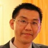
David Keng, Phd, Cla Email & Phone Number
Senior Manager Sustaining and Advanced Manufacturing Engineering
at
Cambridge Technology, a Novanta Company
2 work emails found
@cambridgetechnology.com
LinkedIn matched
✓ Verified July 2026
4 data sources
Profile completeness 100%
Current company
Role
Senior Manager Sustaining and Advanced Manufacturing Engineering
Location
Burlington, Massachusetts, United States
Company size
Who is David Keng, Phd, Cla? Overview
A concise factual answer block for searchers comparing this professional profile.
Quick answer
David Keng, Phd, Cla is listed as Senior Manager Sustaining and Advanced Manufacturing Engineering at Cambridge Technology, a Novanta Company, a with 98 employees, based in Burlington, Massachusetts, United States. AeroLeads shows a work email signal at cambridgetechnology.com and a matched LinkedIn profile for David Keng, Phd, Cla.
David Keng, Phd, Cla previously worked as Manager Sustaining & Advance Manufacturing Engineering at Cambridge Technology, A Novanta Company and Manager Value Add Value Engineering at Cambridge Technology, A Novanta Company. David Keng, Phd, Cla holds Doctor Of Philosophy (Phd), Biomedical/Medical Engineering from Polytechnic Institute Of Nyu.
Company email context
Email format at Cambridge Technology, a Novanta Company
This section adds company-level context without repeating David Keng, Phd, Cla's masked contact details.
*@cambridgetechnology.com
74% confidence
AeroLeads found 2 current-domain work email signals for David Keng, Phd, Cla. Compare company email patterns before reaching out.
Profile bio
About David Keng, Phd, Cla
David Keng, Phd, Cla is a Senior Manager Sustaining and Advanced Manufacturing Engineering at Cambridge Technology, a Novanta Company. He possess expertise in automation, labview, testing, sensors, r&d and 31 more skills.
Listed skills include Automation, Labview, Testing, Sensors, and 32 others.
Current workplace
David Keng, Phd, Cla's current company
Company context helps verify the profile and gives searchers a useful next step.
Cambridge Technology, A Novanta Company
11 roles
David Keng, Phd, Cla work experience
A career timeline built from the work history available for this profile.
Manager Sustaining & Advance Manufacturing Engineering
Current
Apr 2024 - Present
Manager Value Add Value Engineering
Feb 2021 - Apr 2024
Manager System And Software Test Engineering
Apr 2018 - Feb 2021
Senior Principal Qc Engineer
In charge of quality of Asian marketDirect customer facing for any QC related issuesTesting and automationProcess improvementProduct failure analysis
Apr 2016 - Apr 2018
Research Scientist
Current
Microparticle Photophysics Lab
On going fundamental and applied research... Pushing the world record for unlabeled bio-sensing. (currently at the 0.1 atto-grams, single protein level)12 publications with 1000+ citations, work highlighted in Nature and presented in ACS, IAVI, CLEO, PIERS and many other places.Train and guide 15+ MS and PhD students in inter-disciplinary research (EE / ChemE / Physics)Research, Design, Develop the world's most sensitive bio-sensor, single protein sensitivity (0.1 atto- gram sensitivity in water)Design & Program & Build LabVIEW based instrumentation & filtering algorithm for systematic & (semi)automated & versatile experimental research and data analysisDesign & build DFB photonic laser system with <0.1fm RMS stablity with a relative wide scan range (2nm) using hybrid current and temperature tuningFully automatic laser calibration system with a GPIB & LabVIEW controlled Michelson Interferometer (1pm resolution with 600-1600nm range)Design & build ultra-stable testing rig with active temperature controlled Peltier element (0.01 degree C), vibration isolation optical bench, and custom microscope with CCD cameras Design & build modular and fully disposable PDMS microfulidics system with precision syringe pumps, valves, custom pulsation dampers, filters, and PTFE tubing for ultra sensitive bio-sensing with minimal contamination for single molecule sensitivity research, fully programmable flow rate with touch screen GUIMicro machining with either manual or CNC machines to build custom microfluidic setupsBox instrument (DFB laser driver and temperature controller) prototype: mechanical design, PCB design with OEM NI USB DAQ with <1fm RMS noisePortable water-born pathogen detection biosensor system prototype developed for the Department of Defense
Aug 2002 - Present

Senior Quality Control Engineer
Lead engineer FTIR optical engine production line (20M/yr), direct report to division managersPortable analytical instrument electrical, mechanical, optical, software, algorithm, and system level R&D, engineering, and productionTechnical trouble shoot and root cause analysis, initiating and complete design changes to fix multiple catastrophic failure modes of FTIR optical engines and GEMINI portable FTIR/Raman instrumentMain production engineer in GEMINI (FTIR / Raman) mil spec portable analytical instrumentsOptical engine yield improvements 5x increase from original NPI stateDesign, build and implement automatic test rigs to test water-proof ability of the productRoot cause analysis on failure mode of the product water-proof ability (yield improvement from 30% to 100%)Root cause analysis and resolution on FTIR spectrum defects caused by production contaminantsMechanical and electrical analysis, retrofit invention and procedure to eliminate catastrophic voice coil movement failure in FTIR enginesUsing electrical noise spectral analysis, invented new algorithm design to eliminate false rejection of FTIR scan, drastically improved instrument chemical identification reliabilityMechanical and design analysis, invented new gluing process to eliminate water leakage point and mechanical interference caused by instrument LED light pipesDesign and write automated custom LabVIEW software to streamline product final test (time reduction from 10 min per unit to 20 sec per unit)Invent, design and write data review software allowing all engineers and technicians to view and analyze product test data with 10x time efficiency and link component and unit level dataBig data analysis on all production units to mine production failure trendsElectrical test rig design with custom PCB and software to perform isolated unit level power consumption analysisFully automated run-in test software reducing analysis time from 15 min per unit down to 30 sec
Dec 2014 - Mar 2016
Lead Labview Software Engineer
Self initiated, architectured, and implemented a software platform that allows system engineers and software engineers to communicate hundreds of software deliverables: Reduced the old 3 days process with multiple human errors down to a new 3 minutes process with no errors. A total time saving of >99.9%. Self initiated, architectured, and implemented a streamlined platform for the web user interface using scripting. Allowing non-technical person to edit complex html and css through simple tools.Self initiated, architectured, and implemented automatic tools to configure TCP/IP and USB based data acquisition modules to streamline production configuration. A total time saving of >80% and eliminated human error.Component level analog/digital embedded mix PCB debugging in high profile project with urgent deadlines. Successfully finds the design flaw, proposed, implemented temporary fix, and suggested successful permanent fix.
Oct 2013 - Nov 2014

Consultant, Labview Project Engineer
Automation and instrumentation consulting for ALL industries (semiconductor, energy storage, medical device, telecomm, aerospace defense, food and cosmetics... etc.)Personally lead or involved in large scale projects with major corporations (Bose, Philips, IBM, ASML, HP, ATMI, Petra Solar, Raytheon, Telephonic... etc.)Turnkey electro-mechanical solution provider for automated prototyping, production, and testingProject quoting, time & material management, implementation, documentation, and supportNational Instrument hardware & software (LabVIEW, TestStand) based program solution design, implementation, and trainingCertified LabVIEW Architect (CLA), highest LabVIEW certification possible, <700 issued worldwideCertified Professional Instructor (CPI), right to teach and train National Instrument based software/hardwareForms close bond with customers and provide all necessary support when neededBudget and time management to keep both client and self profitable and satisfiedModular instrumentation selection and system building experience using National Instruments PXI, cDAQ, etc.Various box instrument interfacing, communication protocol setup, and programming (GPIB, SERIAL, I2C, SPI, TCP/IP… etc.)Altium designer PCB design and fab.
Aug 2011 - Sep 2013

Research Scientist And Product Design Engineer
Formulate specialty skin contact adhesive patches with and without actives with multiple patents grantedNew product developed with 50% improved performance with 20% less material cost and 30% reduced production time, allowing 3 (instead of 2) batches of adhesives to be made with in one mixing room shiftProposed process and material improvement that resolved a multi-million production quality issue with high customer satisfactorySelf-trained physical chemistry on polymer chemistry and block-co-polymer chemistryIntroduced scientific method for formulation development by rheological instruments analysis (Rheometer, Differential Scanning Calorimeter) and parametric formulation to optimize performance and cost while minimizing development time and costOversees the entire product development cycle: concept, marketing requirement gathering, design review meetings, note book keeping, formulation, raw material gathering, cost analysis, performance testing and analysis, prototype production, raw material qualification, bio-compatibility testing, 510k clearance aid, trial production, QC, full production, production issue debugDesign and build micro-controller (PIC, ATMEL) based instruments and testing rigs for product testing and QC (mechanical, electrical, and pneumatics), IQ/OQ/PQ documentation and approvalProduction line improvement and debugging for both new and existing productIntroduced and modified table-top CNC machines for rapid prototype mold development and reduced prototyping time by >80% with superior qualityAutomated weighing station by connecting the lab scale with RS232 and LabVIEW, reduced the testing time by >80% and eliminated lab notebook hand written errorsR&D department article archive server system, allow all non-regulatory R&D documents (patents, publications, book chapters, competitor's flyers... etc.) to be stored in a central server and index-able and searchable via the system, also allow the users to comment on individual entries
Aug 2009 - May 2011

Visiting Scientist
Technology transfer of WGM bio-sensor, build a research prototype setup, trained NASA technician to operate the setup Setup an entire optical work bench from scratch in working 9 days (laser, laser drivers, fiber optics setup, function generator, detector, PC based DAQ, LabVIEW programming, custom microscope and translation stage... etc.)Train NASA technicians on the basic principle and operation of the prototype setupNegotiate clean room clearance and machine shop clearance to get the basic setup goingDemonstrated detection of CO2 using the prototype setupTrained NASA tech. on fiber etching technique using hydrofluoric acidDocumented the entire setup and the tech. is fully trained
Jun 2004 - Aug 2004
Team & coworkers
Colleagues at Cambridge Technology, a Novanta Company
Other employees you can reach at cambridgetechnology.com. View company contacts for 98 employees →
AE
 Andy Eccles
Colleague at Cambridge Technology, A Novanta CompanyCambridge, Massachusetts, United States
View →
PH
Andy Eccles
Colleague at Cambridge Technology, A Novanta CompanyCambridge, Massachusetts, United States
View →
PH
 Peter Howland
Colleague at Cambridge Technology, A Novanta CompanySudbury, Massachusetts, United States
View →
DE
Peter Howland
Colleague at Cambridge Technology, A Novanta CompanySudbury, Massachusetts, United States
View →
DE
 David E.
Colleague at Cambridge Technology, A Novanta CompanyManchester Area, United Kingdom
View →
KM
David E.
Colleague at Cambridge Technology, A Novanta CompanyManchester Area, United Kingdom
View →
KM
 Kurias Markose
Colleague at Cambridge Technology, A Novanta CompanyIndia
View →
AC
Kurias Markose
Colleague at Cambridge Technology, A Novanta CompanyIndia
View →
AC
 Anthony Crosby
Colleague at Cambridge Technology, A Novanta CompanyNorth Billerica, Massachusetts, United States
View →
GS
Anthony Crosby
Colleague at Cambridge Technology, A Novanta CompanyNorth Billerica, Massachusetts, United States
View →
GS
 Greg Salter
Colleague at Cambridge Technology, A Novanta CompanyTaunton, England, United Kingdom
View →
杨
Greg Salter
Colleague at Cambridge Technology, A Novanta CompanyTaunton, England, United Kingdom
View →
杨
 杨振黄
Colleague at Cambridge Technology, A Novanta CompanySuzhou, Jiangsu, China
View →
KM
杨振黄
Colleague at Cambridge Technology, A Novanta CompanySuzhou, Jiangsu, China
View →
KM
 Karolina Mazur
Colleague at Cambridge Technology, A Novanta CompanyTaunton, England, United Kingdom
View →
WY
Karolina Mazur
Colleague at Cambridge Technology, A Novanta CompanyTaunton, England, United Kingdom
View →
WY
 William Yang
Colleague at Cambridge Technology, A Novanta CompanyShenzhen, Guangdong, China
View →
PB
William Yang
Colleague at Cambridge Technology, A Novanta CompanyShenzhen, Guangdong, China
View →
PB
 Peter Beisecker
Colleague at Cambridge Technology, A Novanta CompanyWaltham, Massachusetts, United States
View →
Peter Beisecker
Colleague at Cambridge Technology, A Novanta CompanyWaltham, Massachusetts, United States
View →
Andy Eccles
Colleague at Cambridge Technology, A Novanta CompanyCambridge, Massachusetts, United States
View →
PH
Peter Howland
Colleague at Cambridge Technology, A Novanta CompanySudbury, Massachusetts, United States
View →
DE
David E.
Colleague at Cambridge Technology, A Novanta CompanyManchester Area, United Kingdom
View →
KM
Kurias Markose
Colleague at Cambridge Technology, A Novanta CompanyIndia
View →
AC
Anthony Crosby
Colleague at Cambridge Technology, A Novanta CompanyNorth Billerica, Massachusetts, United States
View →
GS
Greg Salter
Colleague at Cambridge Technology, A Novanta CompanyTaunton, England, United Kingdom
View →
杨
杨振黄
Colleague at Cambridge Technology, A Novanta CompanySuzhou, Jiangsu, China
View →
KM
Karolina Mazur
Colleague at Cambridge Technology, A Novanta CompanyTaunton, England, United Kingdom
View →
WY
William Yang
Colleague at Cambridge Technology, A Novanta CompanyShenzhen, Guangdong, China
View →
PB
Peter Beisecker
Colleague at Cambridge Technology, A Novanta CompanyWaltham, Massachusetts, United States
View →
3 education records
David Keng, Phd, Cla education
Doctor Of Philosophy (Phd), Biomedical/Medical Engineering
Polytechnic Institute Of Nyu
Master'S Degree, Biomedical Engineering
Polytechnic Institute Of Nyu
Bachelor'S Degree, Electrical And Electronics Engineering
Polytechnic Institute Of Nyu
FAQ
Frequently asked questions about David Keng, Phd, Cla
Quick answers generated from the profile data available on this page.
What company does David Keng, Phd, Cla work for?
David Keng, Phd, Cla works for Cambridge Technology, a Novanta Company.
What is David Keng, Phd, Cla's role at Cambridge Technology, a Novanta Company?
David Keng, Phd, Cla is listed as Senior Manager Sustaining and Advanced Manufacturing Engineering at Cambridge Technology, a Novanta Company.
What is David Keng, Phd, Cla's email address?
AeroLeads has found 2 work email signals at @cambridgetechnology.com for David Keng, Phd, Cla at Cambridge Technology, a Novanta Company.
Where is David Keng, Phd, Cla based?
David Keng, Phd, Cla is based in Burlington, Massachusetts, United States while working with Cambridge Technology, a Novanta Company.
What companies has David Keng, Phd, Cla worked for?
David Keng, Phd, Cla has worked for Cambridge Technology, A Novanta Company, Cambridge Technology, Microparticle Photophysics Lab, Thermo Fisher Scientific, and Nuvera Fuel Cells.
Who are David Keng, Phd, Cla's colleagues at Cambridge Technology, a Novanta Company?
David Keng, Phd, Cla's colleagues at Cambridge Technology, a Novanta Company include Andy Eccles, Peter Howland, David E., Kurias Markose, and Anthony Crosby.
How can I contact David Keng, Phd, Cla?
You can use AeroLeads to view verified contact signals for David Keng, Phd, Cla at Cambridge Technology, a Novanta Company, including work email, phone, and LinkedIn data when available.
What schools did David Keng, Phd, Cla attend?
David Keng, Phd, Cla holds Doctor Of Philosophy (Phd), Biomedical/Medical Engineering from Polytechnic Institute Of Nyu.
What skills is David Keng, Phd, Cla known for?
David Keng, Phd, Cla is listed with skills including Automation, Labview, Testing, Sensors, R&D, Pcb Design, Instrumentation, and Data Acquisition.
Find 750M verified contacts
Search by job title, company, industry, location, and seniority. Export verified B2B contact data when you need it.
Start free trial