AeroLeads people directory · profile
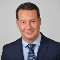
David Van Heerden Email & Phone Number
Director of Process Engineering, Premium Targets
at
Materion Corporation
1 work email found
@materion.com
LinkedIn matched
✓ Verified July 2026
4 data sources
Profile completeness 100%
Current company
Role
Director of Process Engineering, Premium Targets
Location
Baltimore, Maryland, United States
Company size
Who is David Van Heerden? Overview
A concise factual answer block for searchers comparing this professional profile.
Quick answer
David Van Heerden is listed as Director of Process Engineering, Premium Targets at Materion Corporation, a with 1304 employees, based in Baltimore, Maryland, United States. AeroLeads shows a work email signal at materion.com and a matched LinkedIn profile for David Van Heerden.
David Van Heerden previously worked as Global Applications Engineering Manager: Advanced Materials Group at Materion Corporation and Applications Engineer: Advanced Materials Group at Materion Corporation. David Van Heerden holds Phd, Materials Engineering from University Of Cape Town.
Company email context
Email format at Materion Corporation
This section adds company-level context without repeating David Van Heerden's masked contact details.
{first}@materion.com
89% confidence
AeroLeads found 1 current-domain work email signal for David Van Heerden. Compare company email patterns before reaching out.
Profile bio
About David Van Heerden
Solutions-driven engineering leader with a strong customer-centric background and a proven ability to identify and implement innovative solutions to complex technical problems. Able to build dynamic, customer-focused cross-functional teams to develop new products as well as support and enhance existing products. Proven expertise in building customer relationships, identifying new opportunities, and converting them to differentiated successful market solutions.Measurable Career Achievements: - Championed and led the development lifecycle from ideation to qualification and production of a new product line that represents the single largest growth opportunity within the division- Served as the primary technical point of contact for a $300MM materials division, facilitating presentations, technology exchanges, and meetings with customer R&D and engineering groups – creating successful development programs with our largest customers and driving new business- Built a global Applications Engineering team that optimized the customer experience, maximizing engagement possibilities, revenue, and overall satisfaction in service delivery - Developed and led the R&D division for a nanotech startup firm, designing an innovative nanotechnology-based bonding solution that was commercialized and subsequently successfully sold off (and is still in production) I can be reached through LinkedIn or at david_vanheerden@yahoo.com.
Listed skills include Materials Science, R&D, Nanomaterials, Materials, and 46 others.
Current workplace
David Van Heerden's current company
Company context helps verify the profile and gives searchers a useful next step.
Materion Corporation
6 roles
David Van Heerden work experience
A career timeline built from the work history available for this profile.
Global Applications Engineering Manager: Advanced Materials Group
• Provided technical leadership, engineering know-how, and market insight to the identification of new business opportunities as well as the development of new products.• Generated new business opportunities by collaborating with research institutes as well as the R&D groups of large semiconductor fabs. • Lead the development of multiple new products that yielded profitable differentiated market solutions. • Introduced new products to customers and oversaw the qualification and successful scale-up of these materials. Awarded “Materion Growth Champion 2019” in recognition of my efforts. • Provided critical problem-solving skills to troubleshoot production process issues with existing products, thereby increasing yields and resolving customer issues.• Created innovative market extensions of existing products by having a deep understanding of customer products and processes. Extensions included lowering cost of ownership of precious metal and high value targets, enhanced performance by manufacturing process optimization, as well as enhancements to product performance by changes to the product designs. • Established and grew technical relationships with sputter equipment OEMs as well as Materion’s largest semiconductor customers. Became a trusted and valued development partner.• Built a global applications engineering team by identifying and developing high-end talent. The team established deep technical relationships with the R&D and production teams of major semiconductor fabs and identified key opportunities for future growth. • Trained customer engineers and operators on metallurgical and semiconductor aspects of our products, thereby generating customer loyalty and mutual success.• Served as the primary “technical face” of the semiconductor materials products of the Advanced Materials Division, presenting and promoting products at international conferences and trade shows, as well as at Fortune and Global 500 customer technology transfers.
Applications Engineer: Advanced Materials Group
- Established new inroads into customer R&D and technical groups- Raised technical profile of AMG to trusted partner by engaging with customer R&D groups, solving technical issues in their fabs and presenting cutting edge R&D- Provided troubleshooting oversight of PVD functions- Worked closely with customers to develop new processes for materials utilization- Supervised Applications Engineering team, evaluating performance metrics associated with AE workload- Managed usage of existing and emerging products, proactively assessing new proposals prior to submission to the development team
Apr 2013 - Apr 2015
Principal Materials Research Engineer
- Served as the technical lead for the development, qualification, and launch of five new products using NanoMas’ precious-metal-based nanomaterials- Ensured product market strategy effectively communicated and supported long-term objectives- Assessed product performance and identified unique processing techniques, resulting in some of the smallest particle sizes, highest loading, lowest resistivities, and lowest sintering temperatures in the industry- Devised sintering protocols to optimize performance/throughput of nanoparticle conductive traces- Generated a high-performing product development plan aimed at intensifying the vetting process for emerging products- Improved the production of nanoparticle products, resulting in yields increasing from 0% to 90%- Responded to inquiries related to printed electronics and potential opportunities- Developed inks for customer-specific applications- Identified potential market opportunities for NanoMas’ materials
Jan 2010 - Mar 2013
Principal Metallurgist: Thermoelectric Materials And Bonding
Zt Plus
- Established a metallurgical laboratory as well as a powder metallurgy processing facility for the development and production of thermoelectric materials.- Developed brazing and soldering solutions for bonding thermoelectric materials for use in waste heat recovery and cooling applications
Dec 2008 - Dec 2009

Director Of Development Engineering/R&D: Nanomaterials, Pvd, And Bonding
- Led the successful technical transfer and scale-up of NanoFoil® and NanoBond® technology from a university project to volume manufacturable commercial product.- Designed PVD manufacturing equipment for the facility and led the development and scale-up of manufacturing processes.- Recruited and hired the core engineering and production teams and integrated them into a highly functional and effective team. - Directed the development of multiple commercial products: RNT won Nano 50 and R&D 100 awards based on this work and more than 10 patents were filed.- Principal Investigator on more than $10M of government grants and held budgetary responsibility for the research program.
Jan 2004 - Nov 2008
Team & coworkers
Colleagues at Materion Corporation
Other employees you can reach at materion.com. View company contacts for 1304 employees →
CE
 Charlotte Ejiet
Colleague at Materion CorporationNewton Highlands, Massachusetts, United States
View →
YL
Charlotte Ejiet
Colleague at Materion CorporationNewton Highlands, Massachusetts, United States
View →
YL
 Yung Lee
Colleague at Materion CorporationShanghai, China
View →
VM
Yung Lee
Colleague at Materion CorporationShanghai, China
View →
VM
 Victoria Milne, Cpim
Colleague at Materion CorporationElmore, Ohio, United States
View →
SS
Victoria Milne, Cpim
Colleague at Materion CorporationElmore, Ohio, United States
View →
SS
 Sokhantha Sok
Colleague at Materion CorporationTyngsborough, Massachusetts, United States
View →
SB
Sokhantha Sok
Colleague at Materion CorporationTyngsborough, Massachusetts, United States
View →
SB
 Scott Bartlett
Colleague at Materion CorporationFremont, Ohio, United States
View →
GB
Scott Bartlett
Colleague at Materion CorporationFremont, Ohio, United States
View →
GB
 Gary Brown
Colleague at Materion CorporationMaple Heights, Ohio, United States
View →
SY
Gary Brown
Colleague at Materion CorporationMaple Heights, Ohio, United States
View →
SY
 Sherlock Yang
Colleague at Materion CorporationTaichung City, Taiwan, Province Of China
View →
ML
Sherlock Yang
Colleague at Materion CorporationTaichung City, Taiwan, Province Of China
View →
ML
 Ming Li
Colleague at Materion CorporationTokyo, Japan
View →
JJ
Ming Li
Colleague at Materion CorporationTokyo, Japan
View →
JJ
 Jibr J
Colleague at Materion CorporationTyngsborough, Massachusetts, United States
View →
WM
Jibr J
Colleague at Materion CorporationTyngsborough, Massachusetts, United States
View →
WM
 Warren Miller
Colleague at Materion CorporationElyria, Ohio, United States
View →
Warren Miller
Colleague at Materion CorporationElyria, Ohio, United States
View →
Charlotte Ejiet
Colleague at Materion CorporationNewton Highlands, Massachusetts, United States
View →
YL
Yung Lee
Colleague at Materion CorporationShanghai, China
View →
VM
Victoria Milne, Cpim
Colleague at Materion CorporationElmore, Ohio, United States
View →
SS
Sokhantha Sok
Colleague at Materion CorporationTyngsborough, Massachusetts, United States
View →
SB
Scott Bartlett
Colleague at Materion CorporationFremont, Ohio, United States
View →
GB
Gary Brown
Colleague at Materion CorporationMaple Heights, Ohio, United States
View →
SY
Sherlock Yang
Colleague at Materion CorporationTaichung City, Taiwan, Province Of China
View →
ML
Ming Li
Colleague at Materion CorporationTokyo, Japan
View →
JJ
Jibr J
Colleague at Materion CorporationTyngsborough, Massachusetts, United States
View →
WM
Warren Miller
Colleague at Materion CorporationElyria, Ohio, United States
View →
1 education record
David Van Heerden education

FAQ
Frequently asked questions about David Van Heerden
Quick answers generated from the profile data available on this page.
What company does David Van Heerden work for?
David Van Heerden works for Materion Corporation.
What is David Van Heerden's role at Materion Corporation?
David Van Heerden is listed as Director of Process Engineering, Premium Targets at Materion Corporation.
What is David Van Heerden's email address?
AeroLeads has found 1 work email signal at @materion.com for David Van Heerden at Materion Corporation.
Where is David Van Heerden based?
David Van Heerden is based in Baltimore, Maryland, United States while working with Materion Corporation.
What companies has David Van Heerden worked for?
David Van Heerden has worked for Materion Corporation, Nanomas Technologies, Inc., Zt Plus, and Reactive Nanotechnologies.
Who are David Van Heerden's colleagues at Materion Corporation?
David Van Heerden's colleagues at Materion Corporation include Charlotte Ejiet, Yung Lee, Victoria Milne, Cpim, Sokhantha Sok, and Scott Bartlett.
How can I contact David Van Heerden?
You can use AeroLeads to view verified contact signals for David Van Heerden at Materion Corporation, including work email, phone, and LinkedIn data when available.
What schools did David Van Heerden attend?
David Van Heerden holds Phd, Materials Engineering from University Of Cape Town.
What skills is David Van Heerden known for?
David Van Heerden is listed with skills including Materials Science, R&D, Nanomaterials, Materials, Characterization, Pvd, Thin Films, and Failure Analysis.
Find 750M verified contacts
Search by job title, company, industry, location, and seniority. Export verified B2B contact data when you need it.
Start free trialPeople with similar names
Check these profiles if this is not the David Van Heerden you were looking for.
View similar profiles