
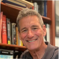
AeroLeads people directory · profile
David Jasinski Email & Phone Number
Math and Science Tutor and Mentor
at
onsemi
1 work email found
@onsemi.com
9 phones found area 585, 858, 716, 508, and 978
LinkedIn matched
✓ Verified July 2026
4 data sources
Profile completeness 100%
Current company
Role
Math and Science Tutor and Mentor
Location
Petaluma, California, United States
Company size
Who is David Jasinski? Overview
A concise factual answer block for searchers comparing this professional profile.
Quick answer
David Jasinski is listed as Math and Science Tutor and Mentor at onsemi, a with 15254 employees, based in Petaluma, California, United States. AeroLeads shows a work email signal at onsemi.com, phone signal with area code 585, 858, 716, 508, 978, and a matched LinkedIn profile for David Jasinski.
David Jasinski previously worked as Retirement at Career Break and Manager Camera Systems at Onsemi. David Jasinski holds M.S., Optics from University Of Rochester.
Company email context
Email format at onsemi
This section adds company-level context without repeating David Jasinski's masked contact details.
{first}.{last}@onsemi.com
89% confidence
AeroLeads found 1 current-domain work email signal for David Jasinski. Compare company email patterns before reaching out.
Profile bio
About David Jasinski
Experienced Systems Engineer and Manager with extensive experience in Optics, Imaging System Architecture Design, Inkjet Printing Systems, Color Management, and Image Processing Algorithm Development.Proven leader in the design of complex imaging systems with meticulous attention to performance optimizationSkilled in calibration procedures and verification methods for Digital Photographic, Electro-photographic, Thermal Dye Sublimation, Inkjet Printers, Transmission Film Scanners, Reflection Print Scanners, and Softcopy Display devicesSuperior command of spatial processing operations and their effect on image structure and quality.Proficient in many methods of Optical System Evaluation: Modulation Transfer Function (MTF) Measurement, Physical and Geometrical Optics, Diffraction Analysis, Radiation PropagationPretty darn good technical collaborator with Singapore, Japan, India and Taiwanese engineers; first-hand experience with manufacturing and end-of-line testing in China
Listed skills include Image Processing, Digital Imaging, Optics, Imaging Science, and 36 others.
Current workplace
David Jasinski's current company
Company context helps verify the profile and gives searchers a useful next step.
Onsemi
10 roles · 43 years
David Jasinski work experience
A career timeline built from the work history available for this profile.
Retirement
Current
Career Break
After 41 years, 10 months and 7 days I've decided to retire from industry and devote my time to helping High School Students in the Petaluma California region improve their Math and Science skills. I am tutoring privately but also as a free service in association with the "Petaluma chapter of the "Mentor Me" program for those students with limited means. My goal is to leverage my experience to demonstrate the relevance of math and science in the Tech Industry. Naturally I welcome any suggestions from former colleagues on current trends, latest science breakthroughs, interesting work anecdotes, etc. that I can pass on to inspire the next crop of engineers.
Mar 2022 - Present
Manager Camera Systems
Coordinate the activities of a very talented group of algorithm development engineers.Set product requirements, performance expectations and schedules.Coach, mentor, support and encourage team members to find creative and cost effective solutions to engineering problems.
Jul 2016 - Mar 2022
Sr. Image Algorithm Engineer
On Semiconductor
Design of image processing algorithm for new and novel sensor architectures with an emphasis on design for hardware implementation.
Jan 2014 - Jan 2016

Image Science Engineer
• Laboratory and field evaluation of a novel CMOS Color Filter Array design• Developed the depth mapping DLL, user interface and optical analysis in support of the development of a depth imaging camera system• Lens shading correction algorithm and compression algorithm analysis and development
2012 - Dec 2014
Adjunct Instructor
Monroe Community College
Tutored Optical, Mechanical and Electrical Engineering students.
2011 - 2012
~1 yr

Senior Engineer
Directed engineers from Rochester, San Diego, Singapore, and Taiwan R.O.C. in the development of scanner firmware. Engineered color tables and sharpening filters for implementation in product firmware.Chaired a multi-disciplinary team of Hardware, Firmware, and Device Driver to ensure subsystem designs conformed to the product’s demanding Image Quality requirements.Mentored manufacturing engineers in Guangzhou China educating them on the proper implementation of end-of-line test procedures.
2003 - 2012
~9 yrs
Image Scientist
Phogenix
As one of eleven founding members of Phogenix (HP/Kodak joint venture), went from start-up to product delivery in three years.Produced the world’s first Inkjet Mini-Lab: Winner of a 2002 Digital Imaging Marketing Association Award for Best Image Quality and Color AccuracyArbitrated between parent companies in leading the development of the Imaging Pipeline.Drove definition of Image Processing, Color Gamut, Tone scale and Inkjet Image Structure requirements. Dictated Writing System performance requirements including specifications for allowable dot gain, dot visibility, banding and implemented the entire system ICC color management platform.
2000 - 2003
~3 yrs
Image System Design
Led software team in the design of the image processing workflow for the first U.S. Digital Photographic Mini-LabDesigned color management and spatial processing to connect an assortment of film scanners, print scanners and digital input sources to a variety of output devices achieving a seamless consistency across these varied platforms.Spearheaded teams driving calibration accuracy and process uniformity to strict tolerances in order to achieve the precision needed to meet image quality goals.
1992 - 2000
~8 yrs
Image Chain Analysis
Kodak Government Systems
Modeled the optical performance of >$1B optical system. Analysis of diffraction performance and radiation propagation ensured maximum utilization of this complex imaging system.Developed, analyzed, and debugged the image processing software for the prototype of a $500M imaging system. Overcame hardware issues in the prototype leading to the invention of a novel calibration method to eliminate artifacts and ensure success of the program. Supervised a group of 10 engineers.
1984 - 1992
~8 yrs
2 education records
David Jasinski education
M.S., Optics
University Of Rochester
B.S., Imaging Science
Rochester Institute Of Technology
FAQ
Frequently asked questions about David Jasinski
Quick answers generated from the profile data available on this page.
What company does David Jasinski work for?
David Jasinski works for onsemi.
What is David Jasinski's role at onsemi?
David Jasinski is listed as Math and Science Tutor and Mentor at onsemi.
What is David Jasinski's email address?
AeroLeads has found 1 work email signal at @onsemi.com for David Jasinski at onsemi.
What is David Jasinski's phone number?
AeroLeads has found 9 phone signal(s) with area code 585, 858, 716, 508, 978 for David Jasinski at onsemi.
Where is David Jasinski based?
David Jasinski is based in Petaluma, California, United States while working with onsemi.
What companies has David Jasinski worked for?
David Jasinski has worked for Onsemi, Career Break, On Semiconductor, Aptina Imaging, and Monroe Community College.
How can I contact David Jasinski?
You can use AeroLeads to view verified contact signals for David Jasinski at onsemi, including work email, phone, and LinkedIn data when available.
What schools did David Jasinski attend?
David Jasinski holds M.S., Optics from University Of Rochester.
What skills is David Jasinski known for?
David Jasinski is listed with skills including Image Processing, Digital Imaging, Optics, Imaging Science, R&D, Digital Image Processing, Inkjet, and Sensors.
Find 750M verified contacts
Search by job title, company, industry, location, and seniority. Export verified B2B contact data when you need it.
Start free trial