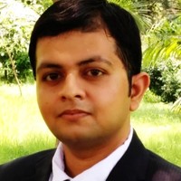
Photonics Researcher
Current
Oct 2023 - Present
Please complete the CAPTCHA to continue
A concise factual answer block for searchers comparing this professional profile.
Deepak Sharma is listed as Researcher at Hitachi R&D | Photonics | AI | MS-EE UTokyo | Semiconductors at Hitachi, a with 3296 employees, based in Kokubunji, Tokyo, Japan. AeroLeads shows a matched LinkedIn profile for Deepak Sharma.
Deepak Sharma previously worked as Photonics Researcher at Hitachi and Graduate Student Researcher at The University Of Tokyo. Deepak Sharma holds Master Of Science - Ms, Electrical Engineering And Information Systems from The University Of Tokyo.
This section adds company-level context without repeating Deepak Sharma's masked contact details.
Review company-level records connected to Deepak Sharma before choosing the right outreach path.
Welcome to my professional profile, where I am pleased to offer a succinct summary of my career journey to date,- Electrical Graduate Student at The University of Tokyo with expertise in semiconductor devices and materials.- Skilled in Device Simulation and Modeling, as well as semiconductor fabrication and characterization- Proficient in programming and scripting languages, utilized for data analysis and visualization in research projects.- Co-authored 4 research articles in international peer-reviewed journals and conferences.- Practical experience in circuit design and modeling gained through a year-long internship at Maxim Integrated Inc.- Experienced in optimizing semiconductor processes, developing novel devices, and collaborating with international researchers.
Company context helps verify the profile and gives searchers a useful next step.
A career timeline built from the work history available for this profile.

Tokyo, Japan
Supervisor: Prof. Masaharu KobayashiResponsibilities:- Conducted independent research on the design and development of FeFET-based memory devices using novel 2D materials such as MoS2, WSe2, WS2, and h-BN.- Optimized the production process of 2D materials, leading to improved material quality and better process yield.- Investigated the ambipolar conductivity of 2D materials and optimized the write/erase performance.Achievements and Outcomes:- Developed over 20 successful devices, demonstrating proficiency in device fabrication and characterization.- Identified Ni/Au electrodes as the optimal choice for achieving ambipolarity in FeFETs through collaboration with researchers from AIST.- Contributed to the optimization of Metal/2D Material interfaces, leading to improved performance of FeFETs.- Made significant contributions to the field of FeFET-based memory devices using 2D materials.Gained:Independent research, Expertise in device fabrication and characterization, Process optimization, Collaboration and teamwork, Problem-solving and analytical skills

Bengaluru, Karnataka, India
Manager: Mr. Tushar PandeyResponsibilities:- Worked collaboratively in a team environment to develop and model high-speed I/O interfaces and package characteristics using the IBIS methodology.- Increased team throughput by creating over 100 IBIS models for use in Signal Integrity (SI) simulations.- Proactively identified, isolated, and resolved complex problems related to SI simulation, demonstrating strong problem-solving ability.- Collaborated with the team to improve model performance and efficiency, and resolved SI-related issues.- Correlated SI simulation and timing analysis with model measurements to complete four projects successfully.- Generated IBIS reports to deliver model measurements and facilitate project analysis.Achievements and Outcomes:- Developed over 100 IBIS models, increasing team throughput and contributing to successful project completion.- Resolved complex SI-related problems and improved model performance and efficiency, resulting in accurate SI simulation and timing analysis.- Correlated SI simulation and timing analysis with model measurements to complete four successful projects.- Built and maintained long-term, mutually beneficial relationships with clients, establishing trust and becoming their go-to resource.Gained: Proficient in the IBIS methodology and SI simulation, Collaborative team player with excellent communication and interpersonal skills, Detail-oriented with exceptional project management and organizational skills.
Mumbai, Maharashtra, India
Supervisor: Prof. Bhaskaran MuralidharanResponsibilities and Achievements:- Researched and implemented a material modeling strategy to device design, resulting in a 30% savings in project budget and reduced costs for growth and fabrication of materials.- Developed band-structure models for Type-II Superlattice Infrared Photodetector using concept of Solid-State Physics and NEGF Methodology based on Quantum-Mechanics.- Implemented the superlattice band structure of bulk InAs and GaSb using an 8-band k.p method with ISRO scientists, boosting the spectral responsivity from 3μm to 30μm.Gained:Expertise in material modeling and design strategy, Knowledge of k.p Hamiltonian Matrix computation and atomistic Non-Equilibrium Green’s Function integration, Ability to propose efficient and optimized designs for specific frequency regimes
Bengaluru, Karnataka, India
Supervisor: Navakanta BhatBachelor Thesis: Steep Slope Sub-Thermionic Conduction in MoS2 FET with a Tunable Transport. Responsibilites and Achievements:- Conducted multiple experiments as a researcher, resulting in the development of a steep slope tunable MoS2 FET.- Developed a novel low power transistor with 2D Material - MoS2 by adopting a T-Shaped Gate design strategy resulting in steep switching (34mV/dec) and high field effect mobility (84.3 cm2V-1s-1).- Fabricated and simulated a dual-gated multilayer MoS2 FET with independent gate control, an optimized Schottky Contact, and a tunable current transport mechanism.- Demonstrated low power consumption and high performance through characterization and TCAD simulation with a correlation of over 85% between modeled data and results.- Published the research findings in the IEEE Transactions on Nanotechnology, indicating the ability to communicate technical work effectively.Gained:Proficient in experimental techniques, including device fabrication and characterization, Expertise in TCAD simulations, Knowledge of 2D materials and their electronic properties, Ability to analyze and interpret data accurately and efficiently, Excellent technical writing and communication skills.

Jabalpur, Madhya Pradesh, India
Supervisor: Prof. Pravin Kondekar and Late Dr. Dheeraj SharmaResponsibilities and Achievements:-Designed energy-efficient FETs for high-speed logic devices using TCAD and physical modeling techniques-Investigated gate metal work function, high-k dielectric, and novel semiconductor materials to improve the subthreshold characteristics of Tunnel FETs-Implemented Poisson and Schrodinger equations based framework for simulation of emerging nanoelectronics devices in TCAD (Silvaco and Sentaurus)- Simulated various types of FETs using the framework to observe the optimized device structure and material process for obtaining steeper switching characteristics (SS < 60mV/decade)- Coordinated and collaborated with Principal Investigators for project proposal, planning, and execution- Published research articles in international journals and presented research papers at international conferences.Gained: Expertise in TCAD simulation, Proficiency in project proposal, planning, and execution, Ability of technical documentation and presenting research papers.
Other employees you can reach at hitachi.com. View company contacts for 3296 employees →
 Andrew Cheah
Colleague at HitachiSingapore
View →
FS
Andrew Cheah
Colleague at HitachiSingapore
View →
FS
 Fatma Siddiqui
Colleague at HitachiMumbai, Maharashtra, India
View →
JJ
Fatma Siddiqui
Colleague at HitachiMumbai, Maharashtra, India
View →
JJ
 Jestin Jose
Colleague at HitachiIbaraki, Japan
View →
EB
Jestin Jose
Colleague at HitachiIbaraki, Japan
View →
EB
 Espen Bye
Colleague at HitachiGreater Oslo Region, Norway
View →
RW
Espen Bye
Colleague at HitachiGreater Oslo Region, Norway
View →
RW
 Rei Wakabayashi
Colleague at HitachiYokohama, Kanagawa, Japan
View →
SK
Rei Wakabayashi
Colleague at HitachiYokohama, Kanagawa, Japan
View →
SK
 Sharath Kumar H A
Colleague at HitachiBengaluru, Karnataka, India
View →
KC
Sharath Kumar H A
Colleague at HitachiBengaluru, Karnataka, India
View →
KC
 Kim Cheng
Colleague at HitachiSan Jose, California, United States
View →
AA
Kim Cheng
Colleague at HitachiSan Jose, California, United States
View →
AA
 Ashraf Ali
Colleague at HitachiDelhi, India
View →
TJ
Ashraf Ali
Colleague at HitachiDelhi, India
View →
TJ
 Tripurari Jha
Colleague at HitachiMumbai, Maharashtra, India
View →
末
Tripurari Jha
Colleague at HitachiMumbai, Maharashtra, India
View →
末
 末永雅士
Colleague at HitachiHitachi, Ibaraki, Japan
View →
末永雅士
Colleague at HitachiHitachi, Ibaraki, Japan
View →
Activities and Societies: Electronics, Robotics, Astronomy
Quick answers generated from the profile data available on this page.
Deepak Sharma works for Hitachi.
Deepak Sharma is listed as Researcher at Hitachi R&D | Photonics | AI | MS-EE UTokyo | Semiconductors at Hitachi.
Deepak Sharma is based in Kokubunji, Tokyo, Japan while working with Hitachi.
Deepak Sharma has worked for Hitachi, The University Of Tokyo, Analog Devices, Indian Institute Of Technology, Bombay, and Indian Institute Of Science (Iisc).
Deepak Sharma's colleagues at Hitachi include Andrew Cheah, Fatma Siddiqui, Jestin Jose, Espen Bye, and Rei Wakabayashi.
You can use AeroLeads to view verified contact signals for Deepak Sharma at Hitachi, including work email, phone, and LinkedIn data when available.
Deepak Sharma holds Master Of Science - Ms, Electrical Engineering And Information Systems from The University Of Tokyo.
Search by job title, company, industry, location, and seniority. Export verified B2B contact data when you need it.
Start free trial Search contactsCheck these profiles if this is not the Deepak Sharma you were looking for.