Role listed
Ibm
Please complete the CAPTCHA to continue
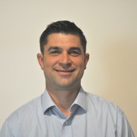
A concise factual answer block for searchers comparing this professional profile.
Derek Summers is listed as Photolithography Engineer at IBM, based in Albany, New York Metropolitan Area, United States. AeroLeads shows a matched LinkedIn profile for Derek Summers.
Derek Summers previously worked as Member of Technical Staff – ASML Equipment Controls/Reticle Engineer, Photolithography at Globalfoundries and Member of Technical Staff - New Technology Development Process Engineer, Photolithography at Globalfoundries. Derek Summers holds Bachelor'S Degree, Microelectronic Engineering from Rochester Institute Of Technology.
This section adds company-level context without repeating Derek Summers's masked contact details.
Review company-level records connected to Derek Summers before choosing the right outreach path.
Derek Summers is a Photolithography Engineer at IBM.
Company context helps verify the profile and gives searchers a useful next step.

A career timeline built from the work history available for this profile.
Albany, Ny, Us
Malta, Ny, Us
Lead, develop and implement improved ASML scanner equipment monitoring controls for dose, focus and overlay performance. Analyze production runtime data to identify opportunities for improvement, including automation and reduced sampling to minimize engineering time and optimize production cycle time. Serve as defect expert for reticle engineers.Created a faster dose monitor for 193nm immersion scanners. Qualified and implemented new photoresist for equipment control monitors leading to $K in cost savings.Managed team to qualify a secondary pellicle supplier for KrF reticles to ensure supply for new product orders.Collaborated with worldwide fabs to benchmark and identify opportunities for reticle creation process improvements.
Malta, Ny, Us
Served as strategist and lead process development engineer. Worked with customers to develop and qualify novel 14nm technology for volume manufacturing, including tool and process technology characterization, troubleshooting and qualification, system and recipe setup and manufacturing. Met with customers daily to review progress and stay on schedule to achieve technology development milestones. Collaborated internally across integration, yield, process modules and metrology engineers for technology qualification. Completed both internal and customer quality documentation for equipment and process qualifications.
Malta, Ny, Us
Served as company representative for EUV equipment factory acceptance. Served as engineer responsible for setup of EUV equipment control automation, recipe integration with factory systems, equipment qualifications and equipment controls.Served as company representative in Veldhoven, Netherlands for factory acceptance of EUV lithography equipment. Drove automation design and testing, including system recipe parameter automation and debugging. Led equipment control automation, including monitoring for line width uniformity.
Malta, Ny, Us
Led a team of lithography unit process engineers responsible for setup, control and optimization of contact/via module lithography processes while managing projects for lean manufacturing opportunities. Managed contact, metal and via process modules for 14nm, 20nm, 28nm, 32nm nodes including lithography equipment and process qualification. Collaborated with process, device and equipment teams to resolve process and tool issues impacting production. Applied lean manufacturing principles to identify and implement new product introduction characterization. Used advanced process control systems to replace manual recipe setup and analysis resulting in time savings equal to 5 full-time engineers. Completed process technology comparison between 20nm and 14nm to realize cross-technology yield benefits and cost savings opportunity of several $ million in chemical and maintenance costs. Led technology development and transfer between development and manufacturing teams. Mentored several college graduates and experienced new hire employees, including process and system training. Trained technicians to manage Statistical Process Control (SPC) setup and maintenance while introducing Fault Detection & Classification (FDC) to reduce mean time and identify process shifts before impacting yield.
Malta, Ny, Us
Served as founding member of photolithography team tasked with start-up of semiconductor Fab 8 facility and first silicon. Transferred and qualified 28nm process technology from Fab 1 Dresden, Germany as well as 32nm process technology from IBM Fishkill. Held residency in Germany to document process specifications and constraints for technology transfer to Malta, New York.Characterized and optimized new resist processes for 20nm, 28nm, 32nm. Utilized Design of Experiments (DOEs) to optimize specifications of contact to gate overlay based on yield and parametric data. Reduced cycle time of lithography equipment install and process qualification. By collaborating with equipment, process integration, metrology, yield teams and executive management to qualify lithography equipment in record time 30d. Collaborated with Optical Proximity Correction (OPC) engineers to build and verify model-based OPC keywords.
Owned and managed front end-of-line photolithography unit process layers. Served as photolithography statistical process control champion to manage and report Process Capability Index (Cpk) performance of internal and key customer specifications. Led team of technicians and operators to oversee reticle inspection and inventory management for ATMC. Qualified new resist processes for 90nm and 130nm node-critical modules. Developed reticle inspection and tracking strategy to reduce the risk of yield limiting reticle defects and reticle inventory. Led acceptance project for KLA STARlight reticle inspection tool from inception to completion.
Served as member of the Research Team responsible for 65nm and 90nm technology research and development. Evaluated Attenuated Phase Shift Mask (APSM), Complementary Phase Shift Mask (CPSM) and Chromeless Phase Lithography (CPL) reticle technologies based on process window, resolution, uniformity and through pitch.Supported process development of contact and via layers on 193nm ASML scanners.Analyzed effects of polysilicon film change based on parametric and yield results.
Brookfield, Ct, Us
Served as member of the Process Development Team with responsibility for 90nm technology. Improved 90nm development photolithography metrology cycle time by 50% by correlating Scanning Electron Microscope (SEM) to optical-based metrology. Optimized SEM recipe design and setup for resolution, linearity, and registration through pitch data collection. Analyzed and reported results to develop and optimize ebeam reticle write processing.
Brookfield, Ct, Us
Served as member of Materials Research Team tasked with materials research and development of novel reticle thin film technology to enable advanced process nodes. Completed factory acceptance and site qualification of a Veeco LDD Ion Beam Deposition Tool. Reduced defect levels and optimized film thickness and optical properties of antireflective chrome and silicon nitride films.

Quick answers generated from the profile data available on this page.
Derek Summers works for IBM.
Derek Summers is listed as Photolithography Engineer at IBM.
Derek Summers is based in Albany, New York Metropolitan Area, United States while working with IBM.
Derek Summers has worked for Ibm, Globalfoundries, Freescale Semiconductor, and Photronics.
You can use AeroLeads to view verified contact signals for Derek Summers at IBM, including work email, phone, and LinkedIn data when available.
Derek Summers holds Bachelor'S Degree, Microelectronic Engineering from Rochester Institute Of Technology.
Search by job title, company, industry, location, and seniority. Export verified B2B contact data when you need it.
Start free trial Search contacts