AeroLeads people directory · profile
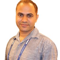
Dinesh Kumar Dixit Email & Phone Number
Principal Project Scientist
at
Indian Institute of Technology, Delhi
LinkedIn matched
✓ Verified August 2026
3 data sources
Profile completeness 86%
Current company
Role
Principal Project Scientist
Location
New Delhi, Delhi, India
Company size
Who is Dinesh Kumar Dixit? Overview
A concise factual answer block for searchers comparing this professional profile.
Quick answer
Dinesh Kumar Dixit is listed as Principal Project Scientist at Indian Institute of Technology, Delhi, a with 7195 employees, based in New Delhi, Delhi, India. AeroLeads shows a matched LinkedIn profile for Dinesh Kumar Dixit.
Dinesh Kumar Dixit previously worked as Senior Project Scientist at Indian Institute Of Technology, Delhi and Research Associate at Indian Institute Of Technology, Delhi. Dinesh Kumar Dixit holds Doctor Of Philosophy - Ph.D., Physics, 8.2/10 from Indian Institute Of Technology, Bombay.
Company email context
Email format at Indian Institute of Technology, Delhi
This section adds company-level context without repeating Dinesh Kumar Dixit's masked contact details.
Indian Institute of Technology, Delhi
Review company-level records connected to Dinesh Kumar Dixit before choosing the right outreach path.
Profile bio
About Dinesh Kumar Dixit
Experienced scientist with a demonstrated history of working in the field of Spintronics, Magnetism and Low Temperature Physics. Expertise in setting up, operation and maintenance of advanced characterization techniques i.e., X-Ray Diffractometer, Profilometer, Atomic Force Microscope, Physical Property Measurement System (PPMS), MPMS SQUID magnetometer etc. Also experienced in Clean room device fabrication. Strong research background with Doctor of Philosophy (Ph.D.) focused on the fabrication and characterization of Spintronics devices from Indian Institute of Technology Bombay.
Current workplace
Dinesh Kumar Dixit's current company
Company context helps verify the profile and gives searchers a useful next step.
Indian Institute Of Technology, Delhi
9 roles
Dinesh Kumar Dixit work experience
A career timeline built from the work history available for this profile.
Principal Project Scientist
In Central Research Facility, IIT Delhi, I am primarily responsible for set up, operation and maintenance of advanced characterization techniques. In addition, I am also responsible for managing day to day operations of the laboratory.Key tasks:• Characterization of solar cell devices to find their EQE• Electrical characterization of semiconductor devices• Hall effect and Magnetoresistance measurements of materials and devices • Magnetic measurements and analysis of materials• Thermal transport measurements of materials and devices• Data interpretation and analysis • Failure analysis of semiconductor devices • Setting up, maintenance and operation of advanced characterization techniques i.e., PPMS, Photovoltaic Characterization (PVE 300), Thermal evaporator system, Glove Box, Solar Simulator, Water Purification System etc.• Collaboration with equipment vendors for installation and maintenance of advanced characterization techniques • Collaboration with cross-functional research teams for material and device characterization• Training students and staff on advanced characterization techniques• Managing and coordinating day to day lab operations• Managing and coordinating internal as well as external users, understanding user requirements and to plan experiments accordingly • Promptly responding to the characterization needs of the users• Contacting vendors for quotations and procurement of lab items• Manuscript reviewing and editing
Senior Project Scientist
At Central Research Facility (CRF), IIT Delhi, my major responsibility was related to operation and maintenance of advanced characterization techniques.Key tasks:• Electrical characterization of semiconductor devices • Vibrating Sample Magnetometer (VSM) measurements of magnetic samples• AC and DC Resistivity measurements of semiconductor devices • AC Susceptibility measurements of magnetic samples • Specific Heat measurements of samples • Seebeck Coefficient measurements of thermoelectric sample• High Impedance measurements of highly resistive samples• Hall measurements of the semiconducting samples and devices• Hall measurements using LCC20 probe• Training students and staff on advanced characterization techniques • Management of day to day operations of the laboratory • Collaboration with equipment vendors for installation, training and maintenance of advanced characterization techniques• Procurement of lab items• Manuscript reviewing and editing
Oct 2019 - Nov 2021
Research Associate
In the lab of Prof. P. K. Muduli (Physics), I worked on Spintronics devices.Key tasks:• Fabrication of thin films using Pulsed Laser Deposition (EXCEL Instruments) and metal sputtering system (AJA International)• Writing LabVIEW programs for equipment interfacing• FMR measurements on thin film samples
Nov 2018 - Jul 2019

Postdoctoral Research Fellow
In Department of Physics, NCKU, in the lab of Professor L. J. Chang, I worked on growth and characterization of superconducting materials and highly frustrated magnetic materials. We had collaborations with different research groups from ANSTO (Australia), RIKEN (Japan), University of Warwick (the UK), ISIS (the UK), PSI (Switzerland) and NCKU (Taiwan) itself. I gained experience working in a collaborative environment and working on multiple projects simultaneously.Key tasks:• Single crystal growth of multiferroic materials using flux method i.e., Eu(x)Sn(1-x)Mn2O5• Growth of superconducting materials i.e., Sc5Ru6Sn18• Characterization of superconducting materials using advanced characterization techniques i.e., XRD, PPMS, SQUID, MuSR etc.• Single crystal orientation using Laue Diffractometer (Photonic Science, the UK)• Data interpretation and analysis • Manuscript writing and submission• Writing research proposals
Oct 2015 - Sep 2018
Research Associate
In this position in the Department of Physics, IIT Bombay, I continued my Ph.D. research work.Key tasks:• Lab scale processing of Si wafers• Clean room fabrication of thin film samples for FMR measurements • Deposition of thin films using PLD, E-beam evaporator and metal sputtering system • Electrical characterization of Spintronics devices• Operation of Atomic Force Microscope (AFM)• Operation of Profilometer for thin film thickness • Operation of advanced characterization techniques i.e., XRD, PPMS, SQUID magnetometer, SEM etc.• Manuscript writing and submission.
Apr 2015 - Oct 2015
Research Scholar
Thesis title: Spintronics Oscillator Based on Magnetic Field Feedback Advisors: Prof. C. V. Tomy and Prof. Ashwin TulapurkarDuring my Ph.D. research in the Department of Physics, IITB, I worked in the field of Spintronics and nanomagnetism. I was involved in the device fabrication and characterization work. For most of my research work I worked in IITB Nanofabrication Facility (IITB-NF) housed in the Department of Electrical Engineering. Our research group (Prof. Ashwin Tulapurkar's group) also had collaborations with Osaka University and AIST, Japan for our device design and fabrication.Key tasks:• Setting up RF probe station set up for electrical characterization of Spintronics oscillator devices • Fabrication of Spintronics devices based on Magnetic Tunnel Junction (MTJ)• Proposing a new circuit design of the Spintronics oscillator based on magnetic field feedback • Electrical characterization of the oscillator devices using RF probe station • Noise studies of the oscillator devices • Thin film deposition using PLD (He-Ne laser) and metal sputtering system (Nordiko) for FMR studies • Lithography of devices using Photolithography (Double Side Aligner) and E-Beam Lithography (RAITH150 TWO)• Imaging the thin films using Scanning Electron Microscope (SEM) and Tunneling Electron Microscope (TEM) and Atomic Force Microscope (AFM)• Surface studies and failure analysis of thin film devices using SIMS and XPS• Measuring thin film thickness using Profilometer• Manuscript writing and submission
Jan 2010 - Apr 2015
Teaching Assistant
I was a TA in B.Tech. 1st year lab during my Ph.D.
Jan 2011 - Dec 2014

Visiting Researcher
While being a Ph.D. student in IIT Bombay, I visited Osaka University for performing experiments on feeback spintronic oscillator device in the lab of Prof. Yoshishize Suzuki.Key tasks:• Electrical characterization of Spintronics feedback oscillator devices using RF probe station• Data interpretation and analysis
Feb 2011 - Mar 2011
3 education records
Dinesh Kumar Dixit education
Doctor Of Philosophy - Ph.D., Physics, 8.2/10

Master'S Degree In Science - Msc, Phyiscs, Distinction
Bachelor'S Degree In Science - Bsc, Physics, Distinction
FAQ
Frequently asked questions about Dinesh Kumar Dixit
Quick answers generated from the profile data available on this page.
What company does Dinesh Kumar Dixit work for?
Dinesh Kumar Dixit works for Indian Institute of Technology, Delhi.
What is Dinesh Kumar Dixit's role at Indian Institute of Technology, Delhi?
Dinesh Kumar Dixit is listed as Principal Project Scientist at Indian Institute of Technology, Delhi.
Where is Dinesh Kumar Dixit based?
Dinesh Kumar Dixit is based in New Delhi, Delhi, India while working with Indian Institute of Technology, Delhi.
What companies has Dinesh Kumar Dixit worked for?
Dinesh Kumar Dixit has worked for Indian Institute Of Technology, Delhi, National Cheng Kung University, Indian Institute Of Technology, Bombay, and Osaka University.
How can I contact Dinesh Kumar Dixit?
You can use AeroLeads to view verified contact signals for Dinesh Kumar Dixit at Indian Institute of Technology, Delhi, including work email, phone, and LinkedIn data when available.
What schools did Dinesh Kumar Dixit attend?
Dinesh Kumar Dixit holds Doctor Of Philosophy - Ph.D., Physics, 8.2/10 from Indian Institute Of Technology, Bombay.
Find 750M verified contacts
Search by job title, company, industry, location, and seniority. Export verified B2B contact data when you need it.
Start free trialPeople with similar names
Check these profiles if this is not the Dinesh Kumar Dixit you were looking for.
View similar profiles
