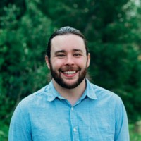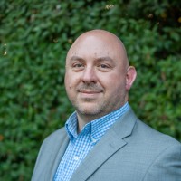

Daniel Baumbach
AeroLeads people directory · profile

Daniel Baumbach Email & Phone Number

Expert in Failure Analysis, Helios Dual Beam Focused Ion Beam Microscopes, and Precision Circuit Edit | Collaborative Team Communicator at Intel Corporation
Location: Galt, California, United States 4 work roles 1 school
LinkedIn matched
✓ Verified August 2026 3 data sources Profile completeness 86%

Contact Signals

LinkedIn Profile matched
3 free lookups remaining · No credit card
Current company
Role
Expert in Failure Analysis, Helios Dual Beam Focused Ion Beam Microscopes, and Precision Circuit Edit | Collaborative Team Communicator
Location
Galt, California, United States
Company size

Who is Daniel Baumbach? Overview

A concise factual answer block for searchers comparing this professional profile.

Quick answer

Daniel Baumbach is listed as Expert in Failure Analysis, Helios Dual Beam Focused Ion Beam Microscopes, and Precision Circuit Edit | Collaborative Team Communicator at Intel Corporation, a with 133841 employees, based in Galt, California, United States. AeroLeads shows a matched LinkedIn profile for Daniel Baumbach.

Daniel Baumbach previously worked as Failure Analysis Engineering Technician - NAND Memory at Intel Corporation and Failure Analysis Engineering Technician - Optane Memory Pathfinding at Intel Corporation. Daniel Baumbach holds Crystalline Material Certificate Of Achievement, Electron Microscopy from San Joaquin Delta College.

Company email context

Email format at Intel Corporation

This section adds company-level context without repeating Daniel Baumbach's masked contact details.

Intel Corporation

Review company-level records connected to Daniel Baumbach before choosing the right outreach path.

Profile bio

About Daniel Baumbach

Dedicated and experienced professional with a proven track record in failure analysis, circuit edit, and technical precision. I specialize in unraveling complex technical challenges and effectively communicating solutions within collaborative teams. My journey with Intel has honed my expertise in failure analysis engineering, where I've been responsible for the full physical failure analysis process of NAND memory packaged units. I excel in many techniques such as Focused Ion Beam (FIB) cross-sections and Transmission Electron Microscope (TEM) sample preparation, as well as workshop design and cross-site knowledge sharing.My commitment to continuous learning and adaptability drives me to always strive for technical excellence. I'm passionate about creating solutions that contribute to program development and enhance product yield. Beyond my technical skills, I bring effective communication, a commitment to quality, and a focus on safety to every project.I'm excited about the future and eager to embrace new challenges. Let's connect and explore opportunities to collaborate and make a meaningful impact.

Current workplace

Daniel Baumbach's current company

Company context helps verify the profile and gives searchers a useful next step.

Intel Corporation
Intel Corporation
Expert in Failure Analysis, Helios Dual Beam Focused Ion Beam Microscopes, and Precision Circuit Edit | Collaborative Team Communicator
santa clara, california, united states
Website
Employees
133841
AeroLeads page
4 roles

Daniel Baumbach work experience

A career timeline built from the work history available for this profile.

Failure Analysis Engineering Technician - Nand Memory

Current

Folsom, California, United States

I have taken a leadership role in the complete physical failure analysis process of NAND memory packaged units, with a primary focus on identifying and isolating specific failures. My demonstrated expertise spans various techniques, including:• Helios Dual Beam Focused Ion Beam (FIB): Experienced in performing targeted single bit Dual Beam FIB cross-sections for in-depth analysis. This includes Planar (P-TEM) and X-TEM Transmission Electron Microscope (TEM) sample preparation to identify physical defects.• Proficient in managing High-Value Inventory and Confidential Intellectual Property• Work in Progress (WIP) Management: Created and managed a WIP queue within SharePoint to efficiently track and prioritize ongoing projects.• Knowledge Sharing: Designed and led workshops to share knowledge and techniques with team members, thereby enhancing the capabilities of the laboratory.• IREM/OBIRCH Sample Preparation: Skills in preparing samples for IREM (Infrared Emission Microscopy) and OBIRCH (Optical beam induced resistance change).• Skilled in deprocessing layer by layer through the array and CMOS using topside and backside approaches. This involves a combination of wet chemistry etches, dry reactive-ion etches (RIE), and precision polishing techniques.• Die Isolation: Capable of isolating a single die (35 micron thick) from a multi-die stack while ensuring its functionality remains intact.• Collaborated closely with cross-functional team members to tackle complex memory device failure issues.• Documented and reported findings to contribute to Fab (fabrication) improvement efforts and enhance product yield.My experience and skills are instrumental in achieving a comprehensive understanding of failure analysis and contributing to the improvement of semiconductor device fabrication processes.

Jan 2022 - Present

Failure Analysis Engineering Technician - Optane Memory Pathfinding

Folsom, California, United States

I have a proven track record in the development of Focused Ion Beam (FIB) sample preparation methods, showcasing my skills in writing Best Known Methods (BKMs), creating training documentation, and providing remote cross site training during the Covid shutdowns. My areas of expertise include Transmission Electron Microscopy (TEM) sample preparation of a single memory bit, NAND polysilicon grain size analysis, and the implementation of methods aimed at enhancing FIB sample success rates and throughput times.I am highly skilled in the creation of samples for TEM using a Helios Dual Beam FIB, with a specific focus on preparing targeted single bit 40nm samples for Optane Memory Technology Development and Pathfinding. As a dual beam FIB tool owner, I take on the responsibilities of first-line dual beam FIB troubleshooting, advanced beam alignments, consumable inventory management, and scheduling routine tool maintenance.My dedication and proficiency in FIB and TEM sample preparation are evident in my contributions to optimizing processes, troubleshooting, and maintaining the tools essential for high-quality sample preparation.

Jun 2014 - Jan 2022

Circuit Edit Engineering Technician

Santa Clara, California, United States

I played a crucial role in advancing next-generation server processor development through my expertise in Focused Ion Beam (FIB) circuit edit debug. My responsibilities also included FIB troubleshooting, managing consumable inventory, calibrations, and routine maintenance of essential tools.In addition to my technical work, I thoroughly documented my efforts by generating detailed reports and delivering presentations on circuit edit procedures and experiments. This ensured transparency and knowledge sharing within the team.Furthermore, I conducted in-depth failure analysis of circuit edits using a dual beam FIB, enabling us to identify and address any issues in circuit edits effectively.Overall, my role significantly impacted the development of advanced server processors, and I am committed to furthering such contributions in future endeavors.

May 2012 - Jun 2014

Failure Analysis Intern

San Jose, California, United States

Responsible for conducting a comprehensive failure analysis process on prototype hard disk drives. This process included tasks such as clean room disassembly, thin film media metrology, scanning electron microscope (SEM) imaging with energy-dispersive X-ray spectroscopy (EDS), and focused ion beam (FIB) cross-sectioning. Furthermore, I generated failure analysis reports based on my findings, which were utilized to contribute to the advancement of product development in this field.

Jun 2011 - May 2012
Team & coworkers

Colleagues at Intel Corporation

Other employees you can reach at intel.com. View company contacts for 133841 employees →

1 education record

Daniel Baumbach education

FAQ

Frequently asked questions about Daniel Baumbach

Quick answers generated from the profile data available on this page.

What company does Daniel Baumbach work for?

Daniel Baumbach works for Intel Corporation.

What is Daniel Baumbach's role at Intel Corporation?

Daniel Baumbach is listed as Expert in Failure Analysis, Helios Dual Beam Focused Ion Beam Microscopes, and Precision Circuit Edit | Collaborative Team Communicator at Intel Corporation.

Where is Daniel Baumbach based?

Daniel Baumbach is based in Galt, California, United States while working with Intel Corporation.

What companies has Daniel Baumbach worked for?

Daniel Baumbach has worked for Intel Corporation and Western Digital.

Who are Daniel Baumbach's colleagues at Intel Corporation?

Daniel Baumbach's colleagues at Intel Corporation include Karthik Kandimalla, Edzon Perez, Gail Kochan, Elias Brooks, and Yidnekachew (Yidnek) Mekonnen.

How can I contact Daniel Baumbach?

You can use AeroLeads to view verified contact signals for Daniel Baumbach at Intel Corporation, including work email, phone, and LinkedIn data when available.

What schools did Daniel Baumbach attend?

Daniel Baumbach holds Crystalline Material Certificate Of Achievement, Electron Microscopy from San Joaquin Delta College.

Find 750M verified contacts

Search by job title, company, industry, location, and seniority. Export verified B2B contact data when you need it.

People with similar names

Check these profiles if this is not the Daniel Baumbach you were looking for.

View similar profiles