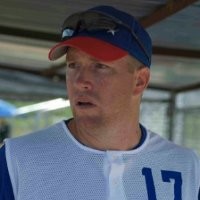

Garrett Standley
AeroLeads people directory · profile

Garrett Standley Email & Phone Number

Lead Electrical Engineer at Honeywell
Location: Lees Summit, Missouri, United States 5 work roles 2 schools
1 work email found @honeywell.com 1 phone found area 512 LinkedIn matched
✓ Verified August 2026 4 data sources Profile completeness 100%

Contact Signals · 1 work email · 1 phone

Work email g****@honeywell.com
Direct phone (512) ***-****
LinkedIn Profile matched
3 free lookups remaining · No credit card
Current company
Role
Lead Electrical Engineer
Location
Lees Summit, Missouri, United States

Who is Garrett Standley? Overview

A concise factual answer block for searchers comparing this professional profile.

Quick answer

Garrett Standley is listed as Lead Electrical Engineer at Honeywell, based in Lees Summit, Missouri, United States. AeroLeads shows a work email signal at honeywell.com, phone signal with area code 512, and a matched LinkedIn profile for Garrett Standley.

Garrett Standley previously worked as Manager Process Engineering at Diodes Inc and Photolithography Engineer at Freescale Semiconductor. Garrett Standley holds Bs, Physices from Texas State University.

Company email context

Email format at Honeywell

This section adds company-level context without repeating Garrett Standley's masked contact details.

{first}.{last}@honeywell.com
86% confidence

AeroLeads found 1 current-domain work email signal for Garrett Standley. Compare company email patterns before reaching out.

Profile bio

About Garrett Standley

Semiconductor engineer with extensive experience in manufacturing, accounting, and management, which are beneficial to organizations who continue to advanced products to customers globally. Skilled in up to date technology and manufacturing processes as well as in overall operations responsibilities. Proven track in record in technical sales abilities to drive organizations to their business objectives.Specialties: SPCPhotolithographyLean ManufacturingKaizen FacilitatorGreen Belt

Listed skills include Semiconductors, Spc, Lean Manufacturing, Photolithography, and 16 others.

Current workplace

Garrett Standley's current company

Company context helps verify the profile and gives searchers a useful next step.

Honeywell
Honeywell
Lead Electrical Engineer
Website
AeroLeads page
5 roles · 35 years

Garrett Standley work experience

A career timeline built from the work history available for this profile.

Lead Electrical Engineer

Current

Charlotte, North Carolina, Us

Daily Activities – Management of the detonator assembly line which includes understanding work flow, dispositioning of NCRs, and verification of process controls in the line.Project Management – Lead the cycle time improvement Kaizen for the chip slapper line. This Kaizen lead to $1.3million in cost savings and a cycle time reduction of 67% over the baseline. The process improvements lead to the first on time delivery of a chip slapper product line since it has been moved to the new location.LTCC Process Improvements – Improved the printing line capacity and yield documentation. Implemented the first SPC systems into the line (for paste thickness) with control and specification limits, and began sharing the data with the DA in order to improve the relationship. Revised the paste qualification SS in order to achieve the PPI buyoff and worked with the DA in order to achieve a correctly documented procedure.Detonator Improvements - Lead the team into the current process of manufacturing. This includes the development of new ways to run the line "lean" in order to make output and also a 71% average reduction in cycle time. Have also lead the team on yield improvement activities improving cable yield to over 55% (from less than 17%), assembly yields increased by an average of 22% across 2 different lines.

Jul 2016 - Present

Manager Process Engineering

Diodes Inc

Daily Activities – Management of the daily activities of 6 engineers. This includes setting the priorities for short and long term projects, daily sustaining duties, and any risk management along with crisis control. This also included covering for any other manager or engineer that off site.Cross Functional Team Leadership – Lead teams of engineers and managers towards the common goal of increased capacity, decreased yield loss, and cost reduction activities. Project Management – Project leader for cross site teams including the change to 8k grit thinning process in order to increase yield, new tool installation to increase site capacity and conversion to 6” wafers, and general process improvement project tracking across the 4 fabrication facilities owned by Diodes.Crisis Management – Assisted the quality team in external customer failures as an expert for facility processing and root cause diagnosis. This included both written and verbal with key quality and management personnel at customer site. This communication included key points for the root cause along with containment and corrective actions.

Nov 2009 - Jul 2016

Photolithography Engineer

Austin, Texas, Us

Troubleshooting of possible scrap, rework, or yield excursions; SPC control of standard qualification tests and production; cycle time and optimum equipment efficiency improvements; determine ways to decrease mean time between failures, and introduction of new cells. Lead multiple chemical minimization projects that have reduced overall resist consumption by more than 30% in less than 1 year resulting in a savings of over $85k per month. Decreased solvent consumption by 12% during the same period for an annual savings $45k. Managed daily inventory of the photolithography chemical budget which was in excess of $4.3million annually. This also encompassed placing new systems (modeling systems) online in order to give more accurate forecasts. Lead the photolithography scrap team during the 2007-2008 time periods and reduced the overall scrap in the area by more than 45% towards a goal of 25%. Major projects included automated recipe verification and on product defectivity monitoring.

Apr 2000 - Nov 2008

Sales Manager

Idi-Cybor Pumps

Key responsibility was for sales and support of the Cybor pumps product line. This included detailed presentations about the Cybor line to high-level customer personnel, negotiation of service contracts and price agreements for the sales contracts. Significant travel was involved during employment due to the large number of systems and a small field service department. Employment was brief due to Cybor being bought out by Roper Industries and relocation wasn’t an option at that time.• Increased sales by 57% over the previous year. Opened 17 new accounts and initiated 25 evaluations in an 8 month period. Worked with external sales representatives in over 20 countries in order to open and improve accounts and service to customers. • Managed 6 engineers that were direct reports and worked on initial demonstrations, evaluations, and installations. This was a global team that operated in Asia, Europe, and North America.

May 1999 - Jun 2000

Photolithography Engineer

Motorola Advanced Products Research Development Lab (Aprdl)

I-line Track tool owner responsibilities include the day to day operations, troubleshooting of any possible scrap or yield excursions, SPC control of qualification tests and production, resist conversions in order to consolidate and/or switch to a leading edge resist, cycle time improvements, and introduction of new cells. • Eliminated the UV Bake tools and saved in excess of $1.2million in under a year due to cycle time, idled tools, and scrap elimination concerns. This included several months of product characterization due to the changes in process.• Lead the photo technician group and was responsible for scheduling weekend coverage, determining project priorities, assigning training and tool owners, and working out minor issues with the staff. Also drove the direction of the photo technicians during staff meetings.

1992 - 1998 ~6 yrs
Team & coworkers

Colleagues at Honeywell

Other employees you can reach at rittal.com. View company contacts →

2 education records

Garrett Standley education

Bs, Physices

Texas State University

Ms, Engineering Management

Walden Universisty
FAQ

Frequently asked questions about Garrett Standley

Quick answers generated from the profile data available on this page.

What company does Garrett Standley work for?

Garrett Standley works for Honeywell.

What is Garrett Standley's role at Honeywell?

Garrett Standley is listed as Lead Electrical Engineer at Honeywell.

What is Garrett Standley's email address?

AeroLeads has found 1 work email signal at @honeywell.com for Garrett Standley at Honeywell.

What is Garrett Standley's phone number?

AeroLeads has found 1 phone signal(s) with area code 512 for Garrett Standley at Honeywell.

Where is Garrett Standley based?

Garrett Standley is based in Lees Summit, Missouri, United States while working with Honeywell.

What companies has Garrett Standley worked for?

Garrett Standley has worked for Honeywell, Diodes Inc, Freescale Semiconductor, Idi-Cybor Pumps, and Motorola Advanced Products Research Development Lab (Aprdl).

Who are Garrett Standley's colleagues at Honeywell?

Garrett Standley's colleagues at Honeywell include Jennifer Encin Druckenmiller, Anton Savenko, Lenhardt László, Glen Herchik, and Jack Beison.

How can I contact Garrett Standley?

You can use AeroLeads to view verified contact signals for Garrett Standley at Honeywell, including work email, phone, and LinkedIn data when available.

What schools did Garrett Standley attend?

Garrett Standley holds Bs, Physices from Texas State University.

What skills is Garrett Standley known for?

Garrett Standley is listed with skills including Semiconductors, Spc, Lean Manufacturing, Photolithography, Process Improvement, Manufacturing, Cross Functional Team Leadership, and Design Of Experiments.

Find 750M verified contacts

Search by job title, company, industry, location, and seniority. Export verified B2B contact data when you need it.