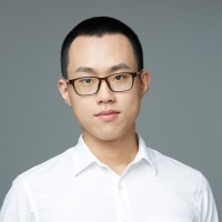
AeroLeads people directory · profile

Geng Chen Email & Phone Number

Principal Failure Analysis Engineer / Senior Manager at HCSemitek Ltd
Location: Jinhua, Zhejiang, China 8 work roles 3 schools
LinkedIn matched
✓ Verified May 2026 3 data sources Profile completeness 86%

Contact Signals

LinkedIn Profile matched
3 free lookups remaining · No credit card
Role
Principal Failure Analysis Engineer / Senior Manager at HCSemitek Ltd
Location
Jinhua, Zhejiang, China

Who is Geng Chen? Overview

A concise factual answer block for searchers comparing this professional profile.

Quick answer

Geng Chen is listed as Principal Failure Analysis Engineer / Senior Manager at HCSemitek Ltd based in Jinhua, Zhejiang, China. AeroLeads shows a matched LinkedIn profile for Geng Chen.

Geng Chen previously worked as 高级经理 at 华灿光电 and Independent Consultant at Independent Consultant. Geng Chen holds Meng, Electrical Engineering from National University Of Singapore.

Profile bio

About Geng Chen

Experienced Professional with a demonstrated history of working in the optoelectronics and semiconuctor industry in China, Singapore and USA. Skilled in Customer Relationship Management, R&D, High Volume Manufacturing, Analytical Skills, LED/PIN/VCSELs/edge-emitting lasers/MEMS/CMOS, Quality Assurance, Failure Analysis and Reliability Engineering.

Listed skills include Failure Analysis, Semiconductors, Reliability, Photovoltaics, and 19 others.

8 roles

Geng Chen work experience

A career timeline built from the work history available for this profile.

高级经理

华灿光电

中国 浙江省 义乌市

Failure analysis on in-house reliability testing and customer complaint/feedback chips, drive for root-cause identifications and containment measures and corrective actions to prevent recurrence; worked as a key member in RED micro LED joint-development team with a key Korean customer, completed successfully Phase I JD activity, signed Phase II development.

Jun 2018 - Mar 2021

Independent Consultant

Chengdu, Sichuan, China

Photovoltaic power plant overall efficiency improvement management: defect detection/prevention; alternative supporting structure evaluation and promotion; PV panel cleaning and maintenance

Sep 2014 - Jun 2018

Sr Manager

Shanghai City, China

Manage the team and provide technical sales support for Key Accounts, Middle East and Africa (MEA) and Americas (NA and SA) regions – set up Company-wide technical training platform and evaluation system; developed Quality management system for JASO overseas JV Fab; lead and represented JASO in cross-company task force including EPC, Lender and Technical.

May 2012 - Aug 2014

Supervisor Engineer, Pv Integration

Sunflux Inc

Fremont, CA

Responsible for leading and driving R&D efforts to improve CdTe/CdS solar cell and module performance from 13% to 16.5% through process window exploration and equipment modification with in-situ thickness monitoring

Jul 2011 - May 2012

Npi R&D Reliability Test Engineer

Milpitas, CA

Responsible for ensuring the reliability of VCSELs, PIN/avalanche photodiodes, DFB edge emitting laser diodes, and Integrated Mach-Zender tunable laser chips – defined reliability testing strategy for chip development, designed and set-up accelerated life test (ALT) process/procedure; analyzed data, predicted and calculated device life-time and.

Feb 2010 - Dec 2010

Team Lead, Dry Etch Process

Santa Clara, CA

Responsible for maintaining, developing, and qualifying RIE processes for digital X-ray image sensor (50x50 cm2) on glass substrates (Mo/Cr Mo-only gate etch, a-Si TFT etch, diode etch, passivation etch) – achieved multi-million-dollar cost-saving new product by qualifying a Mo-only Gate (bottom-gate) etch process within 9 months; timely resolved ESD issue.

Apr 2008 - Jul 2009

Sr R&D Engineer

Intematix

Fremont, CA

Responsible for developing doped-LiFePO4, high-k Dielectric and on-chip integration of wavelength converting Phosphor material/processes utilizing proprietary “Combinatorial” material engineering process

May 2007 - Apr 2008

Principal Engineer

Chartered Semiconductor

Singapore

Responsible for die- and wafer-level failure analysis on advanced CMOS devices: 300-mm Cu 90- nm SOI μ-processor to 200-mm/300-mm 0.13~0.18 μm RF/high-voltage/low-power chips – performed electrical fault isolation using probe-station/curve tracing, liquid crystal analysis, emission microscopy and thermally induced voltage alteration(TIVA); conducted.

May 2006 - May 2007
3 education records

Geng Chen education

FAQ

Frequently asked questions about Geng Chen

Quick answers generated from the profile data available on this page.

What is Geng Chen's role at their current company?

Geng Chen is listed as Principal Failure Analysis Engineer / Senior Manager at HCSemitek Ltd.

Where is Geng Chen based?

Geng Chen is based in Jinhua, Zhejiang, China.

What companies has Geng Chen worked for?

Geng Chen has worked for 华灿光电, Independent Consultant, Ja Solar, Sunflux Inc, and Jds Uniphase.

How can I contact Geng Chen?

You can use AeroLeads to view verified contact signals for Geng Chen, including work email, phone, and LinkedIn data when available.

What schools did Geng Chen attend?

Geng Chen holds Meng, Electrical Engineering from National University Of Singapore.

What skills is Geng Chen known for?

Geng Chen is listed with skills including Failure Analysis, Semiconductors, Reliability, Photovoltaics, Manufacturing, Sensors, Start Ups, and Reliability Engineering.

Find 750M verified contacts

Search by job title, company, industry, location, and seniority. Export verified B2B contact data when you need it.

People with similar names

Check these profiles if this is not the Geng Chen you were looking for.

View similar profiles