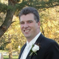

Greg Wald
AeroLeads people directory · profile

Greg Wald Email & Phone Number

Senior Semiconductor Engineer | Process Integration | CMOS Device | Semiconductor Device Characterization | FEOL | NPI | JMP | Communication and Collaboration | Group Problem Solving | Data Mining | JMP
Location: Haymarket, Virginia, United States 9 work roles 2 schools
LinkedIn matched
✓ Verified August 2026 3 data sources Profile completeness 71%

Contact Signals

LinkedIn Profile matched
3 free lookups remaining · No credit card
Role
Senior Semiconductor Engineer | Process Integration | CMOS Device | Semiconductor Device Characterization | FEOL | NPI | JMP | Communication and Collaboration | Group Problem Solving | Data Mining | JMP
Location
Haymarket, Virginia, United States

Who is Greg Wald? Overview

A concise factual answer block for searchers comparing this professional profile.

Quick answer

Greg Wald is listed as Senior Semiconductor Engineer | Process Integration | CMOS Device | Semiconductor Device Characterization | FEOL | NPI | JMP | Communication and Collaboration | Group Problem Solving | Data Mining | JMP based in Haymarket, Virginia, United States. AeroLeads shows a matched LinkedIn profile for Greg Wald.

Greg Wald previously worked as NAND/NOR Process Integration Engineer at Micron Technology and DRAM Process Integration Engineer at Micron Technology. Greg Wald holds Master Of Science - Ms, Electrical Engineering from University Of Missouri-Columbia.

Profile bio

About Greg Wald

Senior Electrical Engineer with extensive experience in creating semiconductor manufacturing solutions. Leverages a background in complex problem solving and project planning to successfully achieve yield, quality, and reliability goals. Develops successful teams and collaboration, enabling technical growth while driving optimal business solutions.

9 roles · 39 years

Greg Wald work experience

A career timeline built from the work history available for this profile.

Nand/Nor Process Integration Engineer

Manassas, Virginia, United States

NAND/NOR Process IntegrationResponsible for CMOS support for 3 FLASH and 1 NOR technology nodes, focus on NOR Automotive capability in last 2 years• Author and co-author on two internal papers regarding process and design improvements to allow for tightening automotive requirements on legacy parts• Key contributor to setup and execution of change business process for addition of Backend tests to Fab test flow• Business process owner for Global Parametric Monitoring System for the Manassas site. Key contributor to Global Parametric Monitoring System change requirements, testing and deployment of new solutions.

Mar 2019 - Feb 2023

Dram Process Integration Engineer

Manassas, Virginia, United States

Responsible for transfer of DRAM CMOS and FEOL technology• Successfully transferred CMOS solution for 4 DRAM designs from Taiwan and 1 design from Japan to Manassas • Empowered CMOS sustaining engineer with recommendations for evaluations and specification changes for the most recent design• Transformed static refresh performance from failing spec to Micron best in class for the technology node

Jan 2018 - Feb 2019

Nand/Nor Process Integration Engineer

Manassas, Virginia, United States

Responsible for transfer of NAND Process flow and CMOS technology• Successfully transferred process flow and CMOS solution for 5 NAND designs from from Singapore to Manassas.• Coordinated PI deliverables for New Part Introduction (NPI) and qualification of all design IDs• Coordinated Manassas FLASH yield predictions and updates to the global business process• CMOS support for High Volume Manufacturing (HVM) – process centering, monitoring and improvements – process equipment qualifications

Jan 2016 - Jun 2018

Nand Process Integration Engineer

Manassas, Virginia, United States

Responsible for transfer of Process flow, FEOL, MOL and CMOS technology of 5 NAND designs from Lehi, UT to Manassas• Successfully transferred process flow and CMOS solution for 5 NAND designs from from Singapore to Manassas.• Coordinated PI deliverables for New Part Introduction (NPI) and qualification of all design IDs• CMOS support for High Volume Manufacturing (HVM) – process centering, monitoring and improvements – process equipment qualifications

Jan 2012 - Jan 2016

Nand Process Integration Engineer

Manassas, Virginia, United States

Responsible for CMOS technology on 300mm NAND• Reduced NAND mask count by two by combining multiple implants on one masking step• Delivered first 300mm site to site parametric benchmarking and monitoring• CMOS support for High Volume Manufacturing (HVM) – process centering, monitoring and improvements – process equipment qualifications

Nov 2008 - Sep 2012

Fab Central Teams Engineer

Manassas, Virginia, United States

Primarily responsible for software solutions for large deviations and change• Delivered system requirements for Global 8 Discipline (G8D) software solution for large deviations. Responsible for ensuring one solution across Wafer Fabrication and Assembly/Test organizations.• Assisted in definition and coordination of Global Change Process (GCP) for wafer fabrication facilities• Assisted FLASH param alignment activity to the Intel-Micron Flash Technology Joint Venture partner.

Oct 2006 - Dec 2008

Senior Engineer

Boise, Idaho, United States

Additional Relevant Experience• Manufacturing Technology Advancement Group• Advanced Device Team – DRAM Transistor Lead• DRAM Transistor and MOL Module Owner• R&D DRAM Process Integration• DRAM Product Engineering• Over 50 patents on semiconductor process and circuits

May 1989 - Sep 2006

Graduate Research Assistant

Columbia, Missouri, United States

Performed Deep Level Transient Spectroscopy (DLTS) to evaluate the following deep level trapso Carbon interstitial and substitutional defects in irradiated Si – resulted in paper o Uniaxial stress effect on the DX center in irradiated Al-GaAs — collaborated on presentation for IPS conference Used equipment existing in lab to set up a second digital DLTS system, doubling analysis capability of the labCoordinated with the machine shop to spec and build a chamber to evaluate Single Event Upset (SEU) on DRAMS

1988 - 1989 ~1 yr

Undergraduate Research Assistant

Columbia, Missouri, United States

Assisted Doctoral students to pull gamma source from reactor and load into collimator, maintain LN2 in germanium detector, alignment of crystals and data collection/plotting.Highlight was testing Mercuric Cadmium Telluride grown on the Space Shuttle versus terrestrial grown.

May 1985 - Aug 1985
2 education records

Greg Wald education

FAQ

Frequently asked questions about Greg Wald

Quick answers generated from the profile data available on this page.

What is Greg Wald's role at their current company?

Greg Wald is listed as Senior Semiconductor Engineer | Process Integration | CMOS Device | Semiconductor Device Characterization | FEOL | NPI | JMP | Communication and Collaboration | Group Problem Solving | Data Mining | JMP.

Where is Greg Wald based?

Greg Wald is based in Haymarket, Virginia, United States.

What companies has Greg Wald worked for?

Greg Wald has worked for Micron Technology and University Of Missouri-Columbia.

How can I contact Greg Wald?

You can use AeroLeads to view verified contact signals for Greg Wald, including work email, phone, and LinkedIn data when available.

What schools did Greg Wald attend?

Greg Wald holds Master Of Science - Ms, Electrical Engineering from University Of Missouri-Columbia.

Find 750M verified contacts

Search by job title, company, industry, location, and seniority. Export verified B2B contact data when you need it.

People with similar names

Check these profiles if this is not the Greg Wald you were looking for.

View similar profiles