
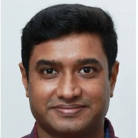
AeroLeads people directory · profile
Hari K Rajeev Email & Phone Number
DFx and Diagnostics Engineer
at
Lattice Semiconductor
1 work email found
@ibm.com
LinkedIn matched
✓ Verified August 2026
4 data sources
Profile completeness 100%
Current company
Role
DFx and Diagnostics Engineer
Location
Georgetown, Penang, Malaysia
Company size
Who is Hari K Rajeev? Overview
A concise factual answer block for searchers comparing this professional profile.
Quick answer
Hari K Rajeev is listed as DFx and Diagnostics Engineer at Lattice Semiconductor, a with 1453 employees, based in Georgetown, Penang, Malaysia. AeroLeads shows a work email signal at ibm.com and a matched LinkedIn profile for Hari K Rajeev.
Hari K Rajeev previously worked as DFx/Diagnostics Engineer at Lattice Semiconductor and Product Development Architect at Intel Corporation. Hari K Rajeev holds B-Tech, Electronics from University Of Kerala.
Company email context
Email format at Lattice Semiconductor
This section adds company-level context without repeating Hari K Rajeev's masked contact details.
{first_initial}{last}@ibm.com
86% confidence
AeroLeads found 1 current-domain work email signal for Hari K Rajeev. Compare company email patterns before reaching out.
Profile bio
About Hari K Rajeev
Highly skilled Design for Test (DFT) engineer with more than 19 years of experience specializing in Test and Scan insertion, test pattern generation, post-silicon bring-up and debug, as well as continuous research on test methodologies and improvements. Recognized for expertise in Scan pattern generation, Verification, and Post-Silicon bring-up and debug.Proven track record of successful test insertion across various ASICs, encompassing test structure verification, JTAG compliance checks, ECO processing, formal verification, and effective customer interaction. Adept in Hierarchical Test Implementation, covering insertion, verification, and test generation processes.Extensive background in Post Silicon bring-up of Automatic Test Pattern Generation (ATPG)/Scan test content in FPGA designs. Notable proficiency in Mentor SSN-based Scan content generation, verification, and Silicon bring-up. Currently engaged in comprehensive DFT implementation, Scan content generation, and post-silicon bring-up of FPGA designs.
Listed skills include Asic, Dft, Vlsi, Static Timing Analysis, and 21 others.
Current workplace
Hari K Rajeev's current company
Company context helps verify the profile and gives searchers a useful next step.
Lattice Semiconductor
8 roles
Hari K Rajeev work experience
A career timeline built from the work history available for this profile.
Jun 2024 - Present

Product Development Architect
-Manufacturing DFx Technical readiness lead for Low End FPGA designs going into the AGILEX3 Series products. -Scan Lead for all Intel FPGA products, responsible for Silicon bring up of the ATPG content, Yield improvement , test time reduction.
Jan 2023 - Jun 2024
Product Development Engineer
Scan Engineer for FPGA chips in the Intel PSG division. - Responsible for development, generation and silicon bring-up of transceiver IP content across 22nm and 16nm nodes. - Worked on developing and bringing up Memory IP ATPG content in the FPGA Core logic for the 14nm product. - Drove Test coverage, test time and yield improvement activities on 20nm,14nm & 10nm FPGA products. - Exploring feasibility to do Cell-Aware ATPG and test methodology improvements for Custom FPGA IPs in the 10nm product line.
Jun 2016 - Dec 2022

Design For Test Engineer For Ibm Power Processor Chips
- Developed Hierarchical Test Methodology for the entire IBM Processor Group.- Worked on developing Hierarchical Test Architecture for new high-end IBM Processor Chip (14nm).- Responsible for Scan Compression architecture and pattern generation for new high-end IBM Processor Chip (14nm).
Apr 2015 - Jun 2016
Senior Staff R&D Engineer
- Instrumental in the migration of the Scan insertion methodology work to Bangalore and setting up a team to continue this work remotely.- Lead the development of an internal LBIST Methodology for OEM ASICs. • Prototyped the generic LBIST Methodology for OEM ASICs • Developed the LBIST insertion Methodology • Driving the LBIST Encounter Test based Scan Verification and Pattern Generation Flow development. • LBIST Execution lead for LBIST insertion, Verification (DRC Checks) and Signature Generation on 2 Large ASIC designs.- Worked on creating BSDL and verifying it against couple of Large Server Designs that were largely 1149-uncompliant.- Nominated to be part of the Talent Sparks community in IBM which is a focus group of high performers.- Developed LBIST Scan patterns and ATPG on Large high-end IBM Processor Chip (22nm)
Jul 2011 - Mar 2015
Staff R&D Engineer
- Drove the effort to architect and develop Scan Insertion Methodology for ASICs in 32nm.- Worked on and made design changes to 2 large Server ASICs to make it 1149-compliant.- Worked on Mentor Graphics (MG) Test Tool Evaluation for OEM ASICs. • Responsible for the evaluation of Scan Insertion, TestKompress insertion and Scan Verification (DRC Checks) and Scan Pattern Generation • Worked with the MG AEs in India and US to create the spec for the utilities and gap analysis.- Imparted ASIC DFT methodology training to many customers, internal designers and new hires.- Received “The Best of IBM! - Eminence and Excellence Award” for outstanding contributions to Systems and Technology group.
Jul 2009 - Jun 2011
Asic Dft Engineer
- Responsible for creating and implementing a test and scan insertion methodology that was used to do scan insertion and test insertion for more than a 100 ASICs- Responsible for the development/maintenance/support of DFT insertion Methodologies in 90nm, 65nm and 45nm. - Drove the effort to develop Out-of-context DFT insertion methodology for ASICs.- Worked in a cross-organization project that studied test compression that we used and based on experimental data on many ASICs, made suggestions to the worldwide design center on optimal fan-out factors
Oct 2004 - Jul 2009
Team & coworkers
Colleagues at Lattice Semiconductor
Other employees you can reach at latticesemi.com. View company contacts for 1453 employees →
LT
 Lenny Thomas
Colleague at Lattice SemiconductorLocust Valley, Pennsylvania, United States
View →
JY
Lenny Thomas
Colleague at Lattice SemiconductorLocust Valley, Pennsylvania, United States
View →
JY
 Jie Yuan
Colleague at Lattice SemiconductorMinhang District, Shanghai, China
View →
MM
Jie Yuan
Colleague at Lattice SemiconductorMinhang District, Shanghai, China
View →
MM
 Marivel M.
Colleague at Lattice SemiconductorDasmariñas, Calabarzon, Philippines
View →
JA
Marivel M.
Colleague at Lattice SemiconductorDasmariñas, Calabarzon, Philippines
View →
JA
 Jordan A.
Colleague at Lattice SemiconductorSalt Lake City Metropolitan Area, United States
View →
YZ
Jordan A.
Colleague at Lattice SemiconductorSalt Lake City Metropolitan Area, United States
View →
YZ
 Yu Zhao
Colleague at Lattice SemiconductorChina
View →
YY
Yu Zhao
Colleague at Lattice SemiconductorChina
View →
YY
 Yuliang Yang
Colleague at Lattice SemiconductorMinhang District, Shanghai, China
View →
YZ
Yuliang Yang
Colleague at Lattice SemiconductorMinhang District, Shanghai, China
View →
YZ
 Yifan Zhou
Colleague at Lattice SemiconductorUnited States
View →
MK
Yifan Zhou
Colleague at Lattice SemiconductorUnited States
View →
MK
 Marc Koe
Colleague at Lattice SemiconductorUnited States
View →
JX
Marc Koe
Colleague at Lattice SemiconductorUnited States
View →
JX
 Jackson Xu
Colleague at Lattice SemiconductorChina
View →
AM
Jackson Xu
Colleague at Lattice SemiconductorChina
View →
AM
 Ave M.
Colleague at Lattice SemiconductorMetro Manila, National Capital Region, Philippines
View →
Ave M.
Colleague at Lattice SemiconductorMetro Manila, National Capital Region, Philippines
View →
Lenny Thomas
Colleague at Lattice SemiconductorLocust Valley, Pennsylvania, United States
View →
JY
Jie Yuan
Colleague at Lattice SemiconductorMinhang District, Shanghai, China
View →
MM
Marivel M.
Colleague at Lattice SemiconductorDasmariñas, Calabarzon, Philippines
View →
JA
Jordan A.
Colleague at Lattice SemiconductorSalt Lake City Metropolitan Area, United States
View →
YZ
Yu Zhao
Colleague at Lattice SemiconductorChina
View →
YY
Yuliang Yang
Colleague at Lattice SemiconductorMinhang District, Shanghai, China
View →
YZ
Yifan Zhou
Colleague at Lattice SemiconductorUnited States
View →
MK
Marc Koe
Colleague at Lattice SemiconductorUnited States
View →
JX
Jackson Xu
Colleague at Lattice SemiconductorChina
View →
AM
Ave M.
Colleague at Lattice SemiconductorMetro Manila, National Capital Region, Philippines
View →
4 education records
Hari K Rajeev education

B-Tech, Electronics
Bachelor'S In Technology, Electrical, Electronics And Communications Engineering
Tkm College Of Engineering

Pre-Degree, Science
High School
Lourde Matha English Medium High School
FAQ
Frequently asked questions about Hari K Rajeev
Quick answers generated from the profile data available on this page.
What company does Hari K Rajeev work for?
Hari K Rajeev works for Lattice Semiconductor.
What is Hari K Rajeev's role at Lattice Semiconductor?
Hari K Rajeev is listed as DFx and Diagnostics Engineer at Lattice Semiconductor.
What is Hari K Rajeev's email address?
AeroLeads has found 1 work email signal at @ibm.com for Hari K Rajeev at Lattice Semiconductor.
Where is Hari K Rajeev based?
Hari K Rajeev is based in Georgetown, Penang, Malaysia while working with Lattice Semiconductor.
What companies has Hari K Rajeev worked for?
Hari K Rajeev has worked for Lattice Semiconductor, Intel Corporation, and Ibm.
Who are Hari K Rajeev's colleagues at Lattice Semiconductor?
Hari K Rajeev's colleagues at Lattice Semiconductor include Lenny Thomas, Jie Yuan, Marivel M., Jordan A., and Yu Zhao.
How can I contact Hari K Rajeev?
You can use AeroLeads to view verified contact signals for Hari K Rajeev at Lattice Semiconductor, including work email, phone, and LinkedIn data when available.
What schools did Hari K Rajeev attend?
Hari K Rajeev holds B-Tech, Electronics from University Of Kerala.
What skills is Hari K Rajeev known for?
Hari K Rajeev is listed with skills including Asic, Dft, Vlsi, Static Timing Analysis, Rtl Design, Atpg, Jtag, and Tcl.
Find 750M verified contacts
Search by job title, company, industry, location, and seniority. Export verified B2B contact data when you need it.
Start free trial