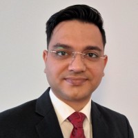
Harshad Mishra
AeroLeads people directory · profile

Harshad Mishra Email & Phone Number

PhD | Quantum Hardware Scientist | Project Leader | Innovating in 3D Integration for the Quantum Leap in Computing at VTT
Location: Espoo, Uusimaa, Finland 5 work roles 3 schools
1 work email found @vtt.fi LinkedIn matched
✓ Verified July 2026 4 data sources Profile completeness 100%

Contact Signals · 1 work email

Work email h****@vtt.fi
LinkedIn Profile matched
3 free lookups remaining · No credit card
Current company
VTT
Role
PhD | Quantum Hardware Scientist | Project Leader | Innovating in 3D Integration for the Quantum Leap in Computing
Location
Espoo, Uusimaa, Finland
Company size

Who is Harshad Mishra? Overview

A concise factual answer block for searchers comparing this professional profile.

Quick answer

Harshad Mishra is listed as PhD | Quantum Hardware Scientist | Project Leader | Innovating in 3D Integration for the Quantum Leap in Computing at VTT, a with 2151 employees, based in Espoo, Uusimaa, Finland. AeroLeads shows a work email signal at vtt.fi and a matched LinkedIn profile for Harshad Mishra.

Harshad Mishra previously worked as Research Scientist at Vtt and Post Doctoral Researcher at Aalto University. Harshad Mishra holds Doctor Of Philosophy - Phd, Physics from Universite De Lorraine.

Company email context

Email format at VTT

This section adds company-level context without repeating Harshad Mishra's masked contact details.

{first}.{last}@vtt.fi
86% confidence

AeroLeads found 1 current-domain work email signal for Harshad Mishra. Compare company email patterns before reaching out.

Profile bio

About Harshad Mishra

Over 12 years of combined experience in MEMS devices and Quantum technologies.Throughout my career, I have worked on several exciting projects. During my MS, I explored the actuation properties of magnetostrictive thin films. For my PhD, I developed a multifunctional magnetic field and temperature sensor based on Surface Acoustic Wave devices, with a potential for significant impact in the field of magnetic field sensing. As a post-doctoral researcher, I investigated the underlying physics behind magnon-phonon interactions. Currently, as a research scientist at VTT Technical Research Center of Finland, I am working on developing TSV technology for quantum processor applications and 3D integration of chips as well as commercial project management.I have extensive experience in nanofabrication, experimental characterizations, simulations, and setting up experiments. Additionally, I am familiar with the principles and fabrication techniques of superconducting circuits and qubits. I have also collaborated with academia and industry, published scientific papers, and mentored students. I have written effective proposals that have been positively reviewed, which demonstrate my ability to identify compelling research questions and design feasible experimental plans. As part of my current role, I am also gaining experience in management of projects - including - project planning, risk analysis and mitigation, as well as E2E project execution.If you are interested in discussing potential opportunities or exploring ways in which we can collaborate, please feel free to reach out to me.

Listed skills include Teaching, Microsoft Word, Data Analysis, Project Management, and 6 others.
Current workplace

Harshad Mishra's current company

Company context helps verify the profile and gives searchers a useful next step.

VTT
Vtt
PhD | Quantum Hardware Scientist | Project Leader | Innovating in 3D Integration for the Quantum Leap in Computing
finland
Website
Employees
2151
AeroLeads page
5 roles

Harshad Mishra work experience

A career timeline built from the work history available for this profile.

Research Scientist

Current
Vtt

Espoo, Uusimaa, Finland

Responsibilities and Experience:1. Leading TSVs and 3D integration technology development for quantum computer applications.2. Nanofabrication process development for multi-stack electrode layers & TSVs.3. Work package and technology lead in multiple XX M€ projects.4. End to end Project Management from initial project justification to final qualification and yield ramp, meeting quality/yield, schedule and cost targets.Primary skills:✓ Electron Beam Lithography✓ UV-Lithography ✓ Thin films deposition – evaporation, sputtering, ALD, CVD✓ Etching – Plasma, Wet, DRIE✓ SEM Microscopy✓ Project Planning & Management

Jan 2023 - Present

Post Doctoral Researcher

Helsinki Area, Finland

My primary task in this job had been to establish a new cryogenic and a room temperature experimental set-up, within the group's existing infrastructure in the Low Temperature Laboratory, for the exploration of magno-mechanical interactions. I also fabricated my own experimental samples at the Micronova and Nanotalo cleanrooms and subsequently conducted measurements on them. Additionally, as part of my duties within the group, I also collaborated with other group members to solve and address any experimental and fabrication roadblocks faced within the group. I was also involved in the development of existing nano-fabrication processes used by the group as well as in the development of new techniques, especially for the fabrication of SAW devices for current and future research projects. I was also involved in supervising interns working within the group. Additionally, I also contributed to the group by innovating new ideas and writing two new project proposals, one of which was also appreciated with the Seal of Excellence by the European Commission.Primary skills:✓ Project Planning✓ Cryogenic experiments✓ Data analysis✓ Electron Beam Lithography✓ Thin films deposition – evaporation, sputtering, ALD✓ Etching – Plasma, Wet✓ SEM Microscopy

Jan 2020 - Dec 2022

Phd Student

Nancy, Grand Est, France

The primary aim of my work was to develop a Surface Acoustic Wave (SAW) device for the detection of magnetic field. The novelty of my work was to implement the physics of shape anisotropy to engineer the SAW device to respond predictably to an applied magnetic field. Another important and unique milestone of my work was the development of an original ‘multi-sensory’ SAW device capable of sensing both magnetic field and temperature, yet independent of each other.During this phase, I was trained in various nanofabrication tools in the cleanroom. I was responsible for the designing and fabrication of my experimental samples as well as for the several experimental measurements to characterize them.Primary Skills:✓ Project Planning & Management✓ Designing of MEMS structures✓ RF Measurements✓ Electron Beam Lithography✓ UV-Lithography ✓ Thin films deposition – evaporation, sputtering, ALD, CVD✓ Etching – Plasma, Wet, DRIE✓ SEM Microscopy

Sep 2016 - Nov 2019

Project Officer

Chennai, Tamil Nadu, India

My primary task during this job was to co-ordinate and develop the research related to magnetostrictive thin films in the Smart Material Characterization lab (at IIT Madras) and train the new students in the related experimental systems. I also established a digital image correlation system (non-contact 2D strain measurement system) in the lab entirely from concept to a fully functional system. I was also involved in assisting Prof. Arockiarajan (PI of the SMC Lab) in writing and finalizing new project proposals and applying for grants.

Mar 2016 - Sep 2016

Project Associate

Chennai, Tamil Nadu, India

My primary task as a project associate was to develop a theoretical understanding and create a modeling tool for the characterization of magnetostrictive thin films. During this phase, I developed a qualitative analysis of deflections in magnetostrictive bi-layers with the aim of optimizing future experimental studies. The study was successfully completed and the report submitted to the funding agency.

Oct 2012 - Jun 2013
Team & coworkers

Colleagues at VTT

Other employees you can reach at vttresearch.com. View company contacts for 2151 employees →

3 education records

Harshad Mishra education

Bachelor Of Technology - Btech, Mechanical Engineering

Institute Of Technical Education And Research
FAQ

Frequently asked questions about Harshad Mishra

Quick answers generated from the profile data available on this page.

What company does Harshad Mishra work for?

Harshad Mishra works for VTT.

What is Harshad Mishra's role at VTT?

Harshad Mishra is listed as PhD | Quantum Hardware Scientist | Project Leader | Innovating in 3D Integration for the Quantum Leap in Computing at VTT.

What is Harshad Mishra's email address?

AeroLeads has found 1 work email signal at @vtt.fi for Harshad Mishra at VTT.

Where is Harshad Mishra based?

Harshad Mishra is based in Espoo, Uusimaa, Finland while working with VTT.

What companies has Harshad Mishra worked for?

Harshad Mishra has worked for Vtt, Aalto University, Institut Jean Lamour (Ijl), and Indian Institute Of Technology, Madras.

Who are Harshad Mishra's colleagues at VTT?

Harshad Mishra's colleagues at VTT include Sanna Haajanen, Alex Minibusssjåfør, Carmen Antuña Rozado, Kauko Immonen, and Nurmi Antti.

How can I contact Harshad Mishra?

You can use AeroLeads to view verified contact signals for Harshad Mishra at VTT, including work email, phone, and LinkedIn data when available.

What schools did Harshad Mishra attend?

Harshad Mishra holds Doctor Of Philosophy - Phd, Physics from Universite De Lorraine.

What skills is Harshad Mishra known for?

Harshad Mishra is listed with skills including Teaching, Microsoft Word, Data Analysis, Project Management, Mems, Research, Microsoft Excel, and Rf Mems.

Find 750M verified contacts

Search by job title, company, industry, location, and seniority. Export verified B2B contact data when you need it.

People with similar names

Check these profiles if this is not the Harshad Mishra you were looking for.

View similar profiles