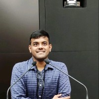
Printed Circuit Board Design Engineer
CurrentPCB designing/ PCB to PCB/ Schematic to PCB/ BOM creation/ Testing/Debugging/Soldering.
Nov 2024 - Present
Please complete the CAPTCHA to continue
A concise factual answer block for searchers comparing this professional profile.
Harshit Gupta is listed as Printed Circuit Board Design Engineer at P2 Power Solutions Pvt. Ltd., a with 86 employees, based in Noida, Uttar Pradesh, India. AeroLeads shows a matched LinkedIn profile for Harshit Gupta.
Harshit Gupta previously worked as District Engineer at Oasys Cybernetics Pvt. Ltd. Harshit Gupta holds Bachelor Of Technology - Btech, Electrical And Electronics Engineering from Mahashi University Of Information Technology.
This section adds company-level context without repeating Harshit Gupta's masked contact details.
Review company-level records connected to Harshit Gupta before choosing the right outreach path.
I am Harshit, equipped with a strong academic foundation in Electronics and Electrical Engineering, complemented by hands-on field experience. I hold a Diploma in Electronics Engineering from JP College, Jahangirabad, and a B.Tech in Electrical Engineering from Maharishi University of Information Technology (MUIT), Noida.Currently, I am working as a PCB Design Engineer in the R&D department of P2 Power Solutions Pvt. Ltd. (November 2024–Present). My role involves designing single and double sided PCBs using advanced EDA tools like Altium Designer and KiCAD. I am proficient in drafting schematics, creating PCB layouts, generating Bills of Materials (BOM), and conducting testing, debugging, and soldering to ensure optimal performance. With expertise in optimizing PCB designs for signal integrity, impedance matching, and high-speed/high-power applications, I ensure adherence to Design for Manufacturability (DFM) and Design for Testability (DFT) guidelines. Additionally, I collaborate with teams across schematic design, planning, manufacturing, and quality assurance to deliver precise and reliable PCB solutionsfor customized products. My specialization in component placement, routing, and ensuring compliance with electrical and mechanical constraints helps minimize crosstalk and achievehigh-performance results.
Company context helps verify the profile and gives searchers a useful next step.
A career timeline built from the work history available for this profile.
Noida, Uttar Pradesh, India
PCB designing/ PCB to PCB/ Schematic to PCB/ BOM creation/ Testing/Debugging/Soldering.

Bulandshahr, Uttar Pradesh, India
Project Coordinator, Project management, Project Engineering, Field Engineer, Site Engineering, Team Player, Technical Support, Customer Support, Site Survey, Operation & Planning, Computer Literacy, Microsoft Office, MS Excel, MS Word, Report Preparation, Maintenance and Repair, English/Hindi Typing, Communication, Electrical/Electronics Engineering, Presentation.
Other employees you can reach at p2power.com. View company contacts for 86 employees →
 Amit Kumar
Colleague at P2 Power Solutions Pvt. Ltd.Greater Delhi Area, India
View →
NL
Amit Kumar
Colleague at P2 Power Solutions Pvt. Ltd.Greater Delhi Area, India
View →
NL
 Neet Lata
Colleague at P2 Power Solutions Pvt. Ltd.Noida, Uttar Pradesh, India
View →
GK
Neet Lata
Colleague at P2 Power Solutions Pvt. Ltd.Noida, Uttar Pradesh, India
View →
GK
 Gunjan Kumar
Colleague at P2 Power Solutions Pvt. Ltd.Noida, Uttar Pradesh, India
View →
SK
Gunjan Kumar
Colleague at P2 Power Solutions Pvt. Ltd.Noida, Uttar Pradesh, India
View →
SK
 Sandeep Kumar
Colleague at P2 Power Solutions Pvt. Ltd.Delhi, India
View →
VC
Sandeep Kumar
Colleague at P2 Power Solutions Pvt. Ltd.Delhi, India
View →
VC
 Vikas Chandra Mishra
Colleague at P2 Power Solutions Pvt. Ltd.Noida, Uttar Pradesh, India
View →
RS
Vikas Chandra Mishra
Colleague at P2 Power Solutions Pvt. Ltd.Noida, Uttar Pradesh, India
View →
RS
 Reetika S.
Colleague at P2 Power Solutions Pvt. Ltd.Delhi, India
View →
DK
Reetika S.
Colleague at P2 Power Solutions Pvt. Ltd.Delhi, India
View →
DK
 Deepak Kumar
Colleague at P2 Power Solutions Pvt. Ltd.Noida, Uttar Pradesh, India
View →
PS
Deepak Kumar
Colleague at P2 Power Solutions Pvt. Ltd.Noida, Uttar Pradesh, India
View →
PS
 Preeti Singh
Colleague at P2 Power Solutions Pvt. Ltd.Noida, Uttar Pradesh, India
View →
SS
Preeti Singh
Colleague at P2 Power Solutions Pvt. Ltd.Noida, Uttar Pradesh, India
View →
SS
 Sanjeev Sharma
Colleague at P2 Power Solutions Pvt. Ltd.Noida, Uttar Pradesh, India
View →
SB
Sanjeev Sharma
Colleague at P2 Power Solutions Pvt. Ltd.Noida, Uttar Pradesh, India
View →
SB
 Sneha Bhati
Colleague at P2 Power Solutions Pvt. Ltd.Noida, Uttar Pradesh, India
View →
Sneha Bhati
Colleague at P2 Power Solutions Pvt. Ltd.Noida, Uttar Pradesh, India
View →

Quick answers generated from the profile data available on this page.
Harshit Gupta works for P2 Power Solutions Pvt. Ltd..
Harshit Gupta is listed as Printed Circuit Board Design Engineer at P2 Power Solutions Pvt. Ltd..
Harshit Gupta is based in Noida, Uttar Pradesh, India while working with P2 Power Solutions Pvt. Ltd..
Harshit Gupta has worked for P2 Power Solutions Pvt. Ltd. and Oasys Cybernetics Pvt. Ltd.
Harshit Gupta's colleagues at P2 Power Solutions Pvt. Ltd. include Amit Kumar, Neet Lata, Gunjan Kumar, Sandeep Kumar, and Vikas Chandra Mishra.
You can use AeroLeads to view verified contact signals for Harshit Gupta at P2 Power Solutions Pvt. Ltd., including work email, phone, and LinkedIn data when available.
Harshit Gupta holds Bachelor Of Technology - Btech, Electrical And Electronics Engineering from Mahashi University Of Information Technology.
Search by job title, company, industry, location, and seniority. Export verified B2B contact data when you need it.
Start free trial Search contactsCheck these profiles if this is not the Harshit Gupta you were looking for.