
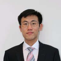
AeroLeads people directory · profile
Haochen Sun Email & Phone Number
Sr. Photolithography Development Engineer
at
Headway Technologies
1 work email found
@headway.com
LinkedIn matched
✓ Verified August 2026
4 data sources
Profile completeness 100%
Current company
Role
Sr. Photolithography Development Engineer
Location
Fremont, California, United States
Company size
Who is Haochen Sun? Overview
A concise factual answer block for searchers comparing this professional profile.
Quick answer
Haochen Sun is listed as Sr. Photolithography Development Engineer at Headway Technologies, a with 385 employees, based in Fremont, California, United States. AeroLeads shows a work email signal at headway.com and a matched LinkedIn profile for Haochen Sun.
Haochen Sun previously worked as Photolithography Process Development Engineer at Headway Technologies and Postdoctoral Researcher at University Of California, Merced. Haochen Sun holds Doctor Of Philosophy - Phd, Chemistry from Washington University In St. Louis.
Company email context
Email format at Headway Technologies
This section adds company-level context without repeating Haochen Sun's masked contact details.
{first}.{last}@headway.com
89% confidence
AeroLeads found 1 current-domain work email signal for Haochen Sun. Compare company email patterns before reaching out.
Profile bio
About Haochen Sun
Knowledgeable and self-motivated process development engineer with rich experience in photolithography, process/prodsuct development, new product ramp up, manufacturability and process stability maintenance, process/product issue identification and troubleshooting, SPC and DOE, as well as data analysis and presentation. I can combine R&D strategy, complex problem solving, project management, team leadership, and cross-disciplinary collaboration to support project & team success.✔️Photolithography process development experience in HDD (PMR/HAMR/TAMR) industry✔️Hands on experiences in semiconductor fabrication tools: ASML 248nm PAS5500 Scanner / Nikon Stepper (i-line, SF-155) / CTDV track / Micralign / SUSS Aligner / AMAT Verity CD SEM / Accent and Inspectrology Overlay / Microscopes / Tencor✔️Develop and Ramp up manufacturable process for 6" and 8" in production line✔️Design down stream process in collaboration with thin film (IBD/CVD) / etching (RIE/IBE) / plating / process integration teams✔️Research experiences: Semiconductor quantum dot materials, 2-dimentional colloidal semiconductor nanocrystals, laser systems alignment and maintenance, photophysical chemistry✔️Charaterization techniques: TEM, HRTEM, EDXS, EELS, SEM, STEM, FIB, ICP-OES, ICP-MS, XPS, XRD, NMR, FT-IR, various Time-Correlated and Static Spectroscopy✔️Software and IT skills: JMP, OriginLab, LabView, C, Python
Listed skills include Material Characterization, Laser, Python, Optics, and 13 others.
Current workplace
Haochen Sun's current company
Company context helps verify the profile and gives searchers a useful next step.
Headway Technologies
6 roles
Haochen Sun work experience
A career timeline built from the work history available for this profile.
Photolithography Process Development Engineer
*PMR/HAMR HDD reader/writer thin-film magnetic recording head device development/fabrication/production Photolithography process development: *Delivered several key layer process for PMR/HAMR HDD writer magnetic recording head design by ASML (248nm) Scanner and i-line Nikon Steppers *Improved key layer within-wafer and wafer-to-wafer CD sigma and lower the overlay residual *Developed and ramped up 8-in wafer production line from start, migrated key writer layers from 6-in production to 8-in line *Served as overlay tool owner for 8-in wafer line, worked with tool vendor for tool qualification and process optimization *Hands-on experience with ASML (248nm) Scanner, i-line Nikon stepper (365nm), AMAT CD-SEM(Verity/Nano/5i/6i), G-line (Micralign, SUSS), Overlay tool (Accent, Inspectrology), Tencor (KLA) *Develop and work on manufacturable process in collaboration with Design, Integration, Thin Film (CVD/IBD), Dry Etch (RIE/IBE), CMP, and Wet Process (electroplating, wet etch) group *Experience working in a high-volume 6” and 8” wafer production line *Extensive experience with SPC (CP/CPK control), DOE, FMEA, and process evaluationsSkills: *Photolithography: ASML PAS 5500, Nikon SF155/i14/i12, Micralign, SUSS Mask aligner, Screen Coater/Developer/inline CTDV track *Metrology: Accent/Inspectrology Overlay, AMAT Verity SEM Nano/5i/6i, FIB, XRD, XRF, AFM, Tencor, Optical Microscopes *Software: SOLID E Simulation, JMP, MATLAB, LabView, VB, C, dw2000, Python

Postdoctoral Researcher
• Investigated the photophysics of InP/ZnSe/ZnS quantum dots and their applications in collaboration with Nanosys, Inc. (Milpitas, CA)• Operated and maintained complex laser systems to measure time-resolved properties of nanocrystals• Published 4 papers
Jun 2021 - Aug 2022

Researcher And Teaching Assistant
• Worked on 5 research projects about the synthesis, shell growth, and surface chemistry of 2-dimensional semiconductor nanocrystal, resulted in 5 research papers (4 first-authored, 1 second-authored)• Taught General Chemistry Lab course for a total of 6 class sections, 120 freshmen students. Received 2016-2017's Teaching Excellence Award• Established efficient chemical precursors and routes for 2D nanocrystal synthesis, shell growth, and surface ligand exchange• Established an optimized protocol for the ICP-OES analysis of semiconductor nanocrystals• Managing the department's FT-IR instrument and software
Aug 2016 - Jan 2021

Undergraduate Research Assistant
• Participated in 2 research projects, and co-authored 2 research papers• Developed the syntheses of cobalt oxide nanocrystals of different morphologies, deposited gold nanoparticles on them, and evaluated their catalytic performances
Jan 2015 - Jun 2016

Undergraduate Research Assistant
• Participated in 1 research project• Helped to develop a rhodium-catalyzed organometallic ring-closing reaction
Aug 2014 - Dec 2014
Team & coworkers
Colleagues at Headway Technologies
Other employees you can reach at headway.com. View company contacts for 385 employees →
JM
 Jayden Martin
Colleague at Headway TechnologiesGranite Bay, California, United States
View →
ID
Jayden Martin
Colleague at Headway TechnologiesGranite Bay, California, United States
View →
ID
 Ibrahim Dursun, Phd
Colleague at Headway TechnologiesMilpitas, California, United States
View →
PY
Ibrahim Dursun, Phd
Colleague at Headway TechnologiesMilpitas, California, United States
View →
PY
 Poua Yang
Colleague at Headway TechnologiesUnited States
View →
DW
Poua Yang
Colleague at Headway TechnologiesUnited States
View →
DW
 Dianna White
Colleague at Headway TechnologiesSan Francisco Bay Area, United States
View →
JB
Dianna White
Colleague at Headway TechnologiesSan Francisco Bay Area, United States
View →
JB
 Jerome Berzuela
Colleague at Headway TechnologiesQuezon City, National Capital Region, Philippines
View →
GL
Jerome Berzuela
Colleague at Headway TechnologiesQuezon City, National Capital Region, Philippines
View →
GL
 Gary Lattus
Colleague at Headway TechnologiesMilpitas, California, United States
View →
SM
Gary Lattus
Colleague at Headway TechnologiesMilpitas, California, United States
View →
SM
 Scott Macdonald
Colleague at Headway TechnologiesSan Jose, California, United States
View →
RE
Scott Macdonald
Colleague at Headway TechnologiesSan Jose, California, United States
View →
RE
 Ramon Edusada
Colleague at Headway TechnologiesMilpitas, California, United States
View →
RD
Ramon Edusada
Colleague at Headway TechnologiesMilpitas, California, United States
View →
RD
 Richard Day
Colleague at Headway TechnologiesSunnyvale, California, United States
View →
YT
Richard Day
Colleague at Headway TechnologiesSunnyvale, California, United States
View →
YT
 Yuhui Tang
Colleague at Headway TechnologiesSan Jose, California, United States
View →
Yuhui Tang
Colleague at Headway TechnologiesSan Jose, California, United States
View →
Jayden Martin
Colleague at Headway TechnologiesGranite Bay, California, United States
View →
ID
Ibrahim Dursun, Phd
Colleague at Headway TechnologiesMilpitas, California, United States
View →
PY
Poua Yang
Colleague at Headway TechnologiesUnited States
View →
DW
Dianna White
Colleague at Headway TechnologiesSan Francisco Bay Area, United States
View →
JB
Jerome Berzuela
Colleague at Headway TechnologiesQuezon City, National Capital Region, Philippines
View →
GL
Gary Lattus
Colleague at Headway TechnologiesMilpitas, California, United States
View →
SM
Scott Macdonald
Colleague at Headway TechnologiesSan Jose, California, United States
View →
RE
Ramon Edusada
Colleague at Headway TechnologiesMilpitas, California, United States
View →
RD
Richard Day
Colleague at Headway TechnologiesSunnyvale, California, United States
View →
YT
Yuhui Tang
Colleague at Headway TechnologiesSan Jose, California, United States
View →
2 education records
Haochen Sun education
Doctor Of Philosophy - Phd, Chemistry
Bachelor Of Science - Bs, Chemistry
FAQ
Frequently asked questions about Haochen Sun
Quick answers generated from the profile data available on this page.
What company does Haochen Sun work for?
Haochen Sun works for Headway Technologies.
What is Haochen Sun's role at Headway Technologies?
Haochen Sun is listed as Sr. Photolithography Development Engineer at Headway Technologies.
What is Haochen Sun's email address?
AeroLeads has found 1 work email signal at @headway.com for Haochen Sun at Headway Technologies.
Where is Haochen Sun based?
Haochen Sun is based in Fremont, California, United States while working with Headway Technologies.
What companies has Haochen Sun worked for?
Haochen Sun has worked for Headway Technologies, University Of California, Merced, Washington University In St. Louis, Nanjing University, and University Of Wisconsin-Madison.
Who are Haochen Sun's colleagues at Headway Technologies?
Haochen Sun's colleagues at Headway Technologies include Jayden Martin, Ibrahim Dursun, Phd, Poua Yang, Dianna White, and Jerome Berzuela.
How can I contact Haochen Sun?
You can use AeroLeads to view verified contact signals for Haochen Sun at Headway Technologies, including work email, phone, and LinkedIn data when available.
What schools did Haochen Sun attend?
Haochen Sun holds Doctor Of Philosophy - Phd, Chemistry from Washington University In St. Louis.
What skills is Haochen Sun known for?
Haochen Sun is listed with skills including Material Characterization, Laser, Python, Optics, Data Analysis, Scanning Electron Microscopy, Spectroscopy, and Inorganic Synthesis.
Find 750M verified contacts
Search by job title, company, industry, location, and seniority. Export verified B2B contact data when you need it.
Start free trialPeople with similar names
Check these profiles if this is not the Haochen Sun you were looking for.
View similar profiles


