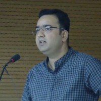
AeroLeads people directory · profile
Jayant Gautam Email & Phone Number
Principal Engineer
at
NXP Semiconductors
1 work email found
@nxp.com
LinkedIn matched
✓ Verified July 2026
4 data sources
Profile completeness 100%
Current company
Role
Principal Engineer
Location
Noida, Uttar Pradesh, India
Company size
Who is Jayant Gautam? Overview
A concise factual answer block for searchers comparing this professional profile.
Quick answer
Jayant Gautam is listed as Principal Engineer at NXP Semiconductors, a with 17460 employees, based in Noida, Uttar Pradesh, India. AeroLeads shows a work email signal at nxp.com and a matched LinkedIn profile for Jayant Gautam.
Jayant Gautam previously worked as Principal Design Engineer at Nxp Semiconductors and Lead Application Engineer at Cadence Design Systems. Jayant Gautam holds M.Tech, Vlsi from North Maharashtra University.
Company email context
Email format at NXP Semiconductors
This section adds company-level context without repeating Jayant Gautam's masked contact details.
{first}.{last}@nxp.com
89% confidence
AeroLeads found 1 current-domain work email signal for Jayant Gautam. Compare company email patterns before reaching out.
Profile bio
About Jayant Gautam
Jayant Gautam is a Principal Engineer at NXP Semiconductors. He possess expertise in place and route, sram, power analysis, low power design, microsoft office and 2 more skills. He is proficient in HINDI. Colleagues describe him as "Jayant was my junior at university. I remember him as a cheerful person. He was attentive and focused in his studies. I wish him the best in his career and personal life." and "Jayant was my junior at university. From day one we got off well. He ably supported me to organise extra curricular activities in college. Even after such a long time we remain in contact with each other and continue to to do so in future. Wish him the best."
Listed skills include Place And Route, Sram, Power Analysis, Low Power Design, and 3 others.
Current workplace
Jayant Gautam's current company
Company context helps verify the profile and gives searchers a useful next step.
Nxp Semiconductors
8 roles
Jayant Gautam work experience
A career timeline built from the work history available for this profile.
Principal Design Engineer

Lead Application Engineer
Worked on Analog Design Environment (ADE),Spectre APS, Spectre X netlists , circuit simulation and mixed signal simulation tools AMS designer, Incisive/Xcelium, Simulation Environment Simvision, Viva ,Statistical analysis Monte Carlo/Corner, Reliability/aging analysis , SPICE/Spectre formats analog/digital design ,Spectre/ SpectreRF analysis – TRAN,DC,AC,PSS, PNOISE
Jan 2019 - Apr 2022
Senior Application Engineer
Worked on Cadence Design Framework (DFII), schematic capture (VSE), Analog Design Environment (ADE) , Analog/Mixed-Signal IC custom layout design, PCELLs , CDFs and Skill Programming LanguageSupport for cadence custom flows, tool development ,installation, Virtuoso Constraints, Modgen
May 2016 - Dec 2018

Consultant Design Engineer
Worked on Core Memory for Global Foundry 14nm using finfet technology.ARXSXXXBNK2KBLP Custom Memory• Worked on 16nm Finfet SRAM(ARXSXXXBNK2KBLP) Memory for AMD India Pvt. Ltd .• Development of Control block & RoutT and RoutB cells with all verifications.• Development & Routing of Slphdr cells with its all verifications.• ECO & Electromigration fixing(EM)
Oct 2014 - Apr 2016

Consultant Design Engineer
1). TSMC 16nm (finfet) ram_llsp122, ram_llsp111Instance level DRC,LVS,ERC, Cell Checker2) . Samsung 14nm finfet ram_sllsp122 Made block ROWDEC from scratch for both compilers ram_sllsp111, ram_sllsp111Done verification for both & control block , Instance level Verifications.3). Generate Lef for custom memories for 14nm & made phase detector for rise & fall and have done all Verifications.4) Worked on 14nm LLPDP Layout editing done for several blocks of Control and IO… Show more 1). TSMC 16nm (finfet) ram_llsp122, ram_llsp111Instance level DRC,LVS,ERC, Cell Checker2) . Samsung 14nm finfet ram_sllsp122 Made block ROWDEC from scratch for both compilers ram_sllsp111, ram_sllsp111Done verification for both & control block , Instance level Verifications.3). Generate Lef for custom memories for 14nm & made phase detector for rise & fall and have done all Verifications.4) Worked on 14nm LLPDP Layout editing done for several blocks of Control and IO Complete LVS/DRC/ERC/Antenna checks/boundry checks verification of physical blocks. Show less
May 2013 - Oct 2014

Graduate Engineer
SYNOPSYS Suite: Galaxy Custom; ,ICV, Hercules 28 nm One port register file Memory Compiler Design 28 nm High Density Two port register file Memory Compiler Design Leafcell Layout Verification Leafcell/Instance level DRC; 28nm High speed one port register file Memory Compiler DesignMiniarray Delievery Leaf cell development,Placement & Routing of Bist I/O cell with DRC,LVS Leafcell DRC/LVS, Instance level DRC, ERC check, chcells extraction and full QA
Dec 2011 - Apr 2013

Project Intern
JOINED Internship Program At DKOP LABS PVT. LTD, During Internship worked in following areas:1). VERILOG, SHELL SCRIPTING2). DIGITAL DESIGN3). DONE PROJECT IN 10GB ETHERNET RECEIVER USING VERILOG4).TCL/TK AND DONE PROJECT EIGHT QUEEN SOLVER
Aug 2010 - May 2011
Team & coworkers
Colleagues at NXP Semiconductors
Other employees you can reach at nxp.com. View company contacts for 17460 employees →
KG
 Kevin Ginter
Colleague at Nxp SemiconductorsGreater Phoenix Area, United States
View →
AL
Kevin Ginter
Colleague at Nxp SemiconductorsGreater Phoenix Area, United States
View →
AL
 Apolonio L. Pitao Jr
Colleague at Nxp SemiconductorsCalabarzon, Philippines
View →
JS
Apolonio L. Pitao Jr
Colleague at Nxp SemiconductorsCalabarzon, Philippines
View →
JS
 Joe Schulze
Colleague at Nxp SemiconductorsGreater Phoenix Area, United States
View →
GD
Joe Schulze
Colleague at Nxp SemiconductorsGreater Phoenix Area, United States
View →
GD
 Greene Deanna
Colleague at Nxp SemiconductorsRockford, Illinois, United States
View →
CK
Greene Deanna
Colleague at Nxp SemiconductorsRockford, Illinois, United States
View →
CK
 Chanyapat Khamkasem
Colleague at Nxp SemiconductorsNakhon Sawan, Thailand
View →
吴
Chanyapat Khamkasem
Colleague at Nxp SemiconductorsNakhon Sawan, Thailand
View →
吴
 吴立宇
Colleague at Nxp SemiconductorsWuhan, Hubei, China
View →
MC
吴立宇
Colleague at Nxp SemiconductorsWuhan, Hubei, China
View →
MC
 Mercer Chiang
Colleague at Nxp SemiconductorsTaipei City, Taiwan, Province Of China
View →
YC
Mercer Chiang
Colleague at Nxp SemiconductorsTaipei City, Taiwan, Province Of China
View →
YC
 Ys Choi
Colleague at Nxp SemiconductorsSeoul Incheon Metropolitan Area, Korea, Republic Of
View →
LM
Ys Choi
Colleague at Nxp SemiconductorsSeoul Incheon Metropolitan Area, Korea, Republic Of
View →
LM
 Lai Marcus
Colleague at Nxp SemiconductorsShah Alam, Selangor, Malaysia
View →
DT
Lai Marcus
Colleague at Nxp SemiconductorsShah Alam, Selangor, Malaysia
View →
DT
 Dilge Terbaş
Colleague at Nxp SemiconductorsEindhoven, North Brabant, Netherlands
View →
Dilge Terbaş
Colleague at Nxp SemiconductorsEindhoven, North Brabant, Netherlands
View →
Kevin Ginter
Colleague at Nxp SemiconductorsGreater Phoenix Area, United States
View →
AL
Apolonio L. Pitao Jr
Colleague at Nxp SemiconductorsCalabarzon, Philippines
View →
JS
Joe Schulze
Colleague at Nxp SemiconductorsGreater Phoenix Area, United States
View →
GD
Greene Deanna
Colleague at Nxp SemiconductorsRockford, Illinois, United States
View →
CK
Chanyapat Khamkasem
Colleague at Nxp SemiconductorsNakhon Sawan, Thailand
View →
吴
吴立宇
Colleague at Nxp SemiconductorsWuhan, Hubei, China
View →
MC
Mercer Chiang
Colleague at Nxp SemiconductorsTaipei City, Taiwan, Province Of China
View →
YC
Ys Choi
Colleague at Nxp SemiconductorsSeoul Incheon Metropolitan Area, Korea, Republic Of
View →
LM
Lai Marcus
Colleague at Nxp SemiconductorsShah Alam, Selangor, Malaysia
View →
DT
Dilge Terbaş
Colleague at Nxp SemiconductorsEindhoven, North Brabant, Netherlands
View →
3 education records
Jayant Gautam education

M.Tech, Vlsi
Master Of Technology; M.Tech
Vlsi Technology
Bachelor Of Technology (B.Tech), Electronics And Communication
FAQ
Frequently asked questions about Jayant Gautam
Quick answers generated from the profile data available on this page.
What company does Jayant Gautam work for?
Jayant Gautam works for NXP Semiconductors.
What is Jayant Gautam's role at NXP Semiconductors?
Jayant Gautam is listed as Principal Engineer at NXP Semiconductors.
What is Jayant Gautam's email address?
AeroLeads has found 1 work email signal at @nxp.com for Jayant Gautam at NXP Semiconductors.
Where is Jayant Gautam based?
Jayant Gautam is based in Noida, Uttar Pradesh, India while working with NXP Semiconductors.
What companies has Jayant Gautam worked for?
Jayant Gautam has worked for Nxp Semiconductors, Cadence Design Systems, Amd, Qualcomm, and Synopsys India Pvt. Ltd.
Who are Jayant Gautam's colleagues at NXP Semiconductors?
Jayant Gautam's colleagues at NXP Semiconductors include Kevin Ginter, Apolonio L. Pitao Jr, Joe Schulze, Greene Deanna, and Chanyapat Khamkasem.
How can I contact Jayant Gautam?
You can use AeroLeads to view verified contact signals for Jayant Gautam at NXP Semiconductors, including work email, phone, and LinkedIn data when available.
What schools did Jayant Gautam attend?
Jayant Gautam holds M.Tech, Vlsi from North Maharashtra University.
What skills is Jayant Gautam known for?
Jayant Gautam is listed with skills including Place And Route, Sram, Power Analysis, Low Power Design, Microsoft Office, Verilog, and Cmos.
Find 750M verified contacts
Search by job title, company, industry, location, and seniority. Export verified B2B contact data when you need it.
Start free trialPeople with similar names
Check these profiles if this is not the Jayant Gautam you were looking for.
View similar profiles