
Technology And Engineering Management Vice-Chair
CurrentI help to connect engineers in the Rochester area to each other in order to learn more about their profession.
Jan 2016 - Present
Please complete the CAPTCHA to continue
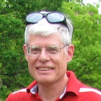
@ieee.org
✓
3 phones found area 585 and 732
✓
LinkedIn matched
A concise factual answer block for searchers comparing this professional profile.
Christopher Cassidy Ph.D. is listed as Technology and Engineering Management vice-chair at IEEE, Rochester Section, a with 1 employees, based in Fairport, New York, United States. AeroLeads shows a work email signal at ieee.org, phone signal with area code 585, 732, and a matched LinkedIn profile for Christopher Cassidy Ph.D..
Christopher Cassidy Ph.D. previously worked as Research, Consulting and Technical Writing at Rochester, Ny and Test Engineer at Binoptics Corporation. Christopher Cassidy Ph.D. holds B.A. Ph.D., Physics from Cornell University.
This section adds company-level context without repeating Christopher Cassidy Ph.D.'s masked contact details.
AeroLeads found 1 current-domain work email signal for Christopher Cassidy Ph.D.. Compare company email patterns before reaching out.
Highly curious research and development professional with a Ph.D. in Physics from Cornell University, and an ability to connect science and technology producers with customers and consumers using clear, concise and compelling scientific and technical writing.I have an extensive background in physics, photonics, optics and imaging science and I am available for writing, research, or consulting projects in these fields.I have an extensive background in physics, photonics, optics and imaging science and I write about physical science, engineering, optics, photonics, MEMS, nano technology and energy at:www.ttoti.blogspot.comI also write about astronomy at:www.semsg.blogspot.comExperience includes:• Work on III-V semiconductor device test and development• Development of electro-optical test systems and methods to measure the optical, electrical, spectral and noise properties of imaging detectors• Work on semiconductor device fabrication and reliability• Characterization of the optical and electrical properties of semiconductor lasers• Team management delivering scan image path software used in multifunction devices• Image path simulation and optimization using Matlab and Xerox imaging software• Familiarity with software development in C, C++ and Perl• Teaching at the university level• Five patentsSpecialties: Specific research and engineering experience in: physics, device development and characterization, optics, imaging, image processing and data analysis. Writing about physical science, engineering, optics, photonics, MEMS, nano technology, and energy.Programming experience in C, C++, Matlab, Java, Perl.
Listed skills include Optics, Sensors, Matlab, Physics, and 18 others.
Company context helps verify the profile and gives searchers a useful next step.
A career timeline built from the work history available for this profile.
Rochester, New York Area
I help to connect engineers in the Rochester area to each other in order to learn more about their profession.
Rochester, Ny
Research, consulting and writing for Physical Sciences, Engineering, Optics, Photonics, MEMS, NanoTechnology, Energy and Environment.
Ithaca, New York Area
Test and development of III-V semiconductor laser devices.

Managed a group of 4 engineers developing the scan image path for use in multifunction products.• Developed image processing parameters and algorithms that enabled the launch of five successful Xerox product families. Successfully implemented image paths optimized to specific scan devices and marking engines on schedule for each product family.• Improved customer satisfaction by resolving problems with scan image quality, file size and scan speed.• Achieved better imaging… Show more Managed a group of 4 engineers developing the scan image path for use in multifunction products.• Developed image processing parameters and algorithms that enabled the launch of five successful Xerox product families. Successfully implemented image paths optimized to specific scan devices and marking engines on schedule for each product family.• Improved customer satisfaction by resolving problems with scan image quality, file size and scan speed.• Achieved better imaging performance than competitive products by defining, simulating, and optimizing tone reproduction, color accuracy, segmentation and compression for Xerox office products.• Produced better image quality at smaller file size than any competitor’s device by integrating mixed raster content compression technology from the Xerox Research Laboratories into product development.• Established product goals by benchmarking image quality of competing devices.• Reduced software defects in products by implementing and maintaining regression testing of scan system imaging software.Engineer, Software and Electronics Development Group• Demonstrated capability to reduce design cycle time by developing discrete event simulation models that accurately predicted memory usage and bandwidth requirements for electrical subsystems. Show less

Rochester, New York Area
Taught courses on Optics, Imaging Science, Mathematics

Senior Research Engineer, Microelectronics Technology Division• Developed two new optical detector arrays for high resolution imaging applications including: An interline transfer device with a refractory metal light shield showing a smear of less than 1% and a full frame device with a lateral overflow drain providing 1000x blooming protection and a transparent conducting gate providing 30% higher sensitivity.• Improved the fabrication yield of imaging detector array devices from 0%… Show more Senior Research Engineer, Microelectronics Technology Division• Developed two new optical detector arrays for high resolution imaging applications including: An interline transfer device with a refractory metal light shield showing a smear of less than 1% and a full frame device with a lateral overflow drain providing 1000x blooming protection and a transparent conducting gate providing 30% higher sensitivity.• Improved the fabrication yield of imaging detector array devices from 0% to commercially viable levels by using process test data, test structure data and final device electrical and optical test data. Located and characterized defects in process and design to improve device yield.• Enabled the production of commercial CMOS devices by qualifying the reliability of the CMOS fabrication processes using measurements of oxide breakdown, electro-migration and hot electron effects. Developed a computer aided test facility to study reliability physics.Process Engineer, Microelectronics Technology Division• Established and maintained manufacturing process control of ion implantation processes. Characterized implant processes by measuring and modeling implant doping profiles in order to understand the effects of defects on semiconductor materials.Research Scientist, Imaging Research Laboratory• Quantified the impact of nonlinear processes on image quality by using a model of the human visual system and models of the image structure properties of imaging systems to study the effect of nonlinear processes on the system modulation transfer function. Member Technical Staff, Kodak Apparatus Division Research Laboratory• Enabled a new laser based printer by characterizing semiconductor lasers and optics to achieve a minimum spot size on the recording surface.• Developed mathematical models to optimize magnetic recording and reading processes. Studied erasure process in magnetic recording systems. Show less

• Initiated and managed a contract research effort to develop an integrated array of high power GaAlAs semiconductor lasers for use in optical recording systems. Developed electro-optical test systems to characterize the optical properties of the semiconductor lasers produced under contract.• Demonstrated a multiple beam optical recording technique capable of increasing optical disk storage density. System used an argon ion laser and a GaAlAs diode laser to reduce mark size on a… Show more • Initiated and managed a contract research effort to develop an integrated array of high power GaAlAs semiconductor lasers for use in optical recording systems. Developed electro-optical test systems to characterize the optical properties of the semiconductor lasers produced under contract.• Demonstrated a multiple beam optical recording technique capable of increasing optical disk storage density. System used an argon ion laser and a GaAlAs diode laser to reduce mark size on a recording surface while requiring less power from the diode laser.• Worked with a team to manage contract development of a high density optical recording system based on metallic media and argon ion laser technology. The team produced one of the first high density optical recording systems. Show less

• Developed a new laser system for the vacuum ultraviolet using a pulsed plasma source and atomic beams. System used a charge exchange.
Achieved a Certificate in Basic Technical Communications. Learned about and practiced different ways of communicating technical information
Quick answers generated from the profile data available on this page.
Christopher Cassidy Ph.D. works for IEEE, Rochester Section.
Christopher Cassidy Ph.D. is listed as Technology and Engineering Management vice-chair at IEEE, Rochester Section.
AeroLeads has found 1 work email signal at @ieee.org for Christopher Cassidy Ph.D. at IEEE, Rochester Section.
AeroLeads has found 3 phone signal(s) with area code 585, 732 for Christopher Cassidy Ph.D. at IEEE, Rochester Section.
Christopher Cassidy Ph.D. is based in Fairport, New York, United States while working with IEEE, Rochester Section.
Christopher Cassidy Ph.D. has worked for Ieee, Rochester Section, Rochester, Ny, Binoptics Corporation, Xerox Corporation, and Rochester Institute Of Technology.
You can use AeroLeads to view verified contact signals for Christopher Cassidy Ph.D. at IEEE, Rochester Section, including work email, phone, and LinkedIn data when available.
Christopher Cassidy Ph.D. holds B.A. Ph.D., Physics from Cornell University.
Christopher Cassidy Ph.D. is listed with skills including Optics, Sensors, Matlab, Physics, Characterization, Digital Imaging, Technical Writing, and Testing.
Search by job title, company, industry, location, and seniority. Export verified B2B contact data when you need it.
Start free trial Search contacts