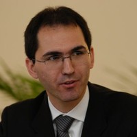
Senior Process Engineer
Current
Oct 2023 - Present
Please complete the CAPTCHA to continue
A concise factual answer block for searchers comparing this professional profile.
Jérôme Nicolas is listed as Senior Process Engineer at ASM, a with 1885 employees, based in Greater Tokyo Area, Japan. AeroLeads shows a matched LinkedIn profile for Jérôme Nicolas.
Jérôme Nicolas previously worked as Process Engineer at Asm and Ph.D. Student in Engineering Physics at Polytechnique Montréal. Jérôme Nicolas holds Engineering Degree, Material Science And Engineering, Master Of Engineering from Insa Rennes.
This section adds company-level context without repeating Jérôme Nicolas's masked contact details.
Review company-level records connected to Jérôme Nicolas before choosing the right outreach path.
Versatile research scientist with a strong background in semiconductors science and a variety of practical experiences in R&D in microfabrication and automated data acquisition.Strong expertise in materials characterization (e.g. structural, electrical and optical properties of semiconductor materials) and fabrication (e.g. chemical vapor deposition). Deep understanding of engineering aspects relative to transistors, diodes, fiber optics and MEMs gained in the field during various academic and professional projects.Efficient team worker demonstrating leadership skills and facilitating communication in between individuals. Capable of communicating efficiently and presenting results clearly. Hard worker and fast learner demonstrating curiosity and autonomy resulting in continuous self-improvement.
Listed skills include Leadership, Semiconductor Device, Optics, Fiber Optics, and 46 others.
Company context helps verify the profile and gives searchers a useful next step.
A career timeline built from the work history available for this profile.

Montreal, Canada Area
CVD growth development and structural characterization of SiGeSn alloys• Analyzed the impact of growth parameters in terms of Sn incorporation, crystalline quality and material stability resulting in a presentation at the joint International SiGe Technology and Device Meeting and International Conference on Silicon Epitaxy and Heterostructures (ICSI-ISTDM) in 2018.• Established the feasibility of mid-IR technology integration on silicon using CMOS-compatible GeSn alloys by demonstrating the first light emission up to 3.5 µm in a collaborative peer-reviewed paper.• Developed tunable strain-relaxed buffer epitaxial layers to enable the coherent growth of high-quality GeSn layers, resulting in 5 collaborative publications in high-impact scientific journals.Research tutor: Oussama Moutanabbirhttp://www.polymtl.ca/nhl/index.php

Paris Area, France
Fabrication and characterization of graphene RF antenna and rectifier• Collaboratively designed the experimental testing procedures of the devices’ fabrication steps leading to the development of a suitable process for graphene patterning.• Designed UV masks and optimized optical and electronic lithography steps to fabricate devices and reach the specifications (dimensions and reproducibility).• Demonstrated creative problem solving leading to the fabrication of graphene RF antenna prototype with tunable signal reception over 130 MHz and established the fabrication guidelines for graphene RF rectifiers with length below 500 nm

London, United Kingdom
Substrate transfer and electrical characterization of 2D materials• Developed a process for the transfer of molybdenum disulfide (MoS2) and tungsten disulfide (WS2) bidimensional layers on insulating substrate for the fabrication of field-effect transistor.• Realized transfer of 15 µm-wide 2-D flakes using a PMMA polymer film with a loss rate below 20%.• Designed a custom-made LabVIEW program to automate the temperature-dependent electrical characterization of transistors in the cryogenic chamber of a four-point probe station, successfully benchmarked on a conductive material

Lyon Area, France
Implementation of optical monitoring sensor and software for automotive joint coating• Collaborated with the production manager and operators to implement the optical system on the production line and conduct the sensor and software tests on real and simulated defects.• Identified all possible defects and the associated sensor responses. Established the sensor position and parameters to achieve the highest sensitivity to these defects.• Developed a LabVIEW software to interface the sensor and detect the manufacturing defects by means of real-time signal analysis
Other employees you can reach at asm.com. View company contacts for 1885 employees →
 Anirudh Dabir
Colleague at AsmTempe, Arizona, United States
View →
DL
Anirudh Dabir
Colleague at AsmTempe, Arizona, United States
View →
DL
 Dongyoung Lee
Colleague at AsmHwaseong, Gyeonggi, South Korea, Korea, Republic Of
View →
HC
Dongyoung Lee
Colleague at AsmHwaseong, Gyeonggi, South Korea, Korea, Republic Of
View →
HC
 Hsin-Yu Chen
Colleague at AsmPhoenix, Arizona, United States
View →
VO
Hsin-Yu Chen
Colleague at AsmPhoenix, Arizona, United States
View →
VO
 Vera Ong
Colleague at AsmSingapore
View →
CK
Vera Ong
Colleague at AsmSingapore
View →
CK
 Chia-Chun Kuo
Colleague at AsmHsinchu City, Taiwan, Province Of China
View →
SB
Chia-Chun Kuo
Colleague at AsmHsinchu City, Taiwan, Province Of China
View →
SB
 Selahattin Bahce
Colleague at AsmTürkiye, Turkey
View →
DA
Selahattin Bahce
Colleague at AsmTürkiye, Turkey
View →
DA
 Diego Alejandro Guzman-Lozano
Colleague at AsmCochabamba, Bolivia, Plurinational State Of
View →
HM
Diego Alejandro Guzman-Lozano
Colleague at AsmCochabamba, Bolivia, Plurinational State Of
View →
HM
 Hoang M. Nguyen
Colleague at AsmHelsinki Metropolitan Area, Finland
View →
JT
Hoang M. Nguyen
Colleague at AsmHelsinki Metropolitan Area, Finland
View →
JT
 Judy Torre
Colleague at AsmEast Haven, Connecticut, United States
View →
KO
Judy Torre
Colleague at AsmEast Haven, Connecticut, United States
View →
KO
 Kt Ooi
Colleague at AsmSingapore
View →
Kt Ooi
Colleague at AsmSingapore
View →

Semiconductors physics Microfabrication techniques Microelectronic devices Optoelectronics Instrumentation Material mechanics

Nanostructured materials Functional materials Corrosion engineering Cementitious and ceramic materials engineering Physical properties.
Quick answers generated from the profile data available on this page.
Jérôme Nicolas works for ASM.
Jérôme Nicolas is listed as Senior Process Engineer at ASM.
Jérôme Nicolas is based in Greater Tokyo Area, Japan while working with ASM.
Jérôme Nicolas has worked for Asm, Polytechnique Montréal, Thales, Imperial College London, and Saint-Gobain Performance Plastics.
Jérôme Nicolas's colleagues at ASM include Anirudh Dabir, Dongyoung Lee, Hsin-Yu Chen, Vera Ong, and Chia-Chun Kuo.
You can use AeroLeads to view verified contact signals for Jérôme Nicolas at ASM, including work email, phone, and LinkedIn data when available.
Jérôme Nicolas holds Engineering Degree, Material Science And Engineering, Master Of Engineering from Insa Rennes.
Jérôme Nicolas is listed with skills including Leadership, Semiconductor Device, Optics, Fiber Optics, Electronics Manufacturing, Research And Development, Material Characterisation, and Integrated Circuits.
Search by job title, company, industry, location, and seniority. Export verified B2B contact data when you need it.
Start free trial Search contactsCheck these profiles if this is not the Jérôme Nicolas you were looking for.
View similar profiles