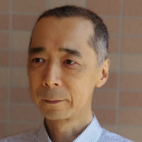

Who is Junichi Kikkawa? Overview
A concise factual answer block for searchers comparing this professional profile.
Quick answer
Junichi Kikkawa is listed as tech lead at HCLTech, based in Yokohama, Kanagawa, Japan. AeroLeads shows a work email signal at xilinx.com and a matched LinkedIn profile for Junichi Kikkawa.
Junichi Kikkawa previously worked as * at 2P Perfect Presentation and Engineer at Synkom Co., Ltd.. Junichi Kikkawa holds Master Of Science Chemical Engineering, Protain Structure Analysis Using X Ray from Nagoya University.
Company email context
Email format at HCLTech
This section adds company-level context without repeating Junichi Kikkawa's masked contact details.
{first}.{last}@xilinx.com
89% confidence
AeroLeads found 2 current-domain work email signals for Junichi Kikkawa. Compare company email patterns before reaching out.
Profile bio
About Junichi Kikkawa
I focused to generate better physical design. faster, smaller, less power.I prefer to work as a stand alone hand-on layout engineer. and as side channel support, I worked as a programmer, AE, methodlogiest, flow integration. As a hand on physical designer in Fujitsu, Simplex and Cadence for - hierarchy or flat P&R for 0.25um, 0.18um, 0.13, 90nm, 65nm.- network QoS, CPU bridge chip, 8 core network processor- ASIC, ASSP, micro controller, Si, GaAs, gatearray, standard cell, Tr level integration.I cover large area of LSI physical designing. in past in Fujitsu, I worked for- router program from scratch- integrate design flow using JCL, sh script. Tcl.- develop the layout approach based on Tr level P & R.- San Jose ASIC design center support manager- lead CAD group as a manager.Good communication skill both Japanese and English.Specialties: I worked for most of major Japanese IDM.- Toshiba, Renesas, Fujitsu, NEC.My strength aprt from physical deign is programing capablity( automation is important quality result)- C, C++ 20+ year, include pthread, socket, X11- AWK,Tcl 10+year- Verilog 3year- Javascript, Pythonusing Linux from 0.98
Listed skills include Tcl, Semiconductors, Fpga, Asic, and 16 others.
Current workplace
Junichi Kikkawa's current company
Company context helps verify the profile and gives searchers a useful next step.
8 roles · 41 years
Junichi Kikkawa work experience
A career timeline built from the work history available for this profile.

Engineer
Synkom do on site time and material service to turn key design, using FPGA and ASIC.Of course, ex-STARC support member work to improve design and design flow.
May 2018 - Nov 2024

Staff Strategic Ae, Manager
supporting local FPGA customer. focus for FPGA synthesis and implementation. The word 'implementation' in FPGA world means- Map to FPGA elements (LUT) of specific chip.- Assign LUT location and select route as wire.
Oct 2009 - May 2018
Firm Software Developer
Self
writing and planing the next stage.- writing a SDIO I/O firm driver for embedded controller. (almost done!. it works)- writing a FAT16 system above on SDIO for SD memory card(open, unlink, link, then write and read) learned the difference between processor + software design vs hardware design.
May 2009 - Oct 2009
Fae
Contractor For Silistix
Mar 2008 - May 2009

Technical Leader
- consulting & hand-on for LSI physical design. flow and design itself.- P&R, STA, physical verification, power grid analysis- C++, Tcl, Verilog RTL. worked with Japanese LSI venders and US fabless companypast project. - a high end computer chip set consult review the design flow. recommand the approach to power mesh analysis. clean up the DRC, LVS and ERC flow - gaming computer bridge chip set layout engineer re-design the power mesh, help floor plan. help them to understand OCV. review random number generator. - SPI4.2 network chip layout designer complete 2 layout block digital layout design. design almost full digital delay lay - HDTV frame convertor chip layout enginner pad assign of flip chip, 2 channel DDR. help HDMI IP integeration.
Aug 2001 - Dec 2008

Manager
CAD software development 1986-1996 - maze method router.US ASIC design center support 1996-2000 - support the design center activity. + help size and cost estimation. + solve design issue, like improve run time, chip size, power consumtions + introduce new design approach, like equivalence check, power mesh analysis, timing driven layout, scan chain re-ordering + help communication to other group. inside Fujitsu, CAD vendor, external design house.Manager of methodology development 2000-2001
1986 - 2001
~15 yrs
1 education record
Junichi Kikkawa education

FAQ
Frequently asked questions about Junichi Kikkawa
Quick answers generated from the profile data available on this page.
What company does Junichi Kikkawa work for?
Junichi Kikkawa works for HCLTech.
What is Junichi Kikkawa's role at HCLTech?
Junichi Kikkawa is listed as tech lead at HCLTech.
What is Junichi Kikkawa's email address?
AeroLeads has found 2 work email signals at @xilinx.com for Junichi Kikkawa at HCLTech.
Where is Junichi Kikkawa based?
Junichi Kikkawa is based in Yokohama, Kanagawa, Japan while working with HCLTech.
What companies has Junichi Kikkawa worked for?
Junichi Kikkawa has worked for Hcltech, 2P Perfect Presentation, Synkom Co., Ltd., Xilinx, and Self.
How can I contact Junichi Kikkawa?
You can use AeroLeads to view verified contact signals for Junichi Kikkawa at HCLTech, including work email, phone, and LinkedIn data when available.
What schools did Junichi Kikkawa attend?
Junichi Kikkawa holds Master Of Science Chemical Engineering, Protain Structure Analysis Using X Ray from Nagoya University.
What skills is Junichi Kikkawa known for?
Junichi Kikkawa is listed with skills including Tcl, Semiconductors, Fpga, Asic, Static Timing Analysis, Embedded Systems, Verilog, and Rtl Design.
Find 750M verified contacts
Search by job title, company, industry, location, and seniority. Export verified B2B contact data when you need it.
Start free trialPeople with similar names
Check these profiles if this is not the Junichi Kikkawa you were looking for.
View similar profiles