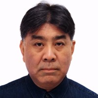
代表
Current
ナノアート・プロジェクト
CMP を始めとする超精密加工技術の研究開発に関する技術コンサルテーションを業務としている。さらに、先端技術の研究開発マネジメント、技術者教育、技術文書の翻訳 等さまざまな業務に関してサポート可能である。
Apr 2016 - Present
Please complete the CAPTCHA to continue
A concise factual answer block for searchers comparing this professional profile.
Keiichi Kimura is listed as ナノアート・プロジェクト - 代表 at ナノアート・プロジェクト, based in Fukuoka, Japan. AeroLeads shows a matched LinkedIn profile for Keiichi Kimura.
Keiichi Kimura previously worked as 代表 at ナノアート・プロジェクト and 教授 at 国立 台湾科技大学 機械工程系. Keiichi Kimura holds 工学学士, 精密工学 from 北海道大学 工学部 精密工学科.
Keiichi Kimura is a ナノアート・プロジェクト - 代表 at ナノアート・プロジェクト.
Company context helps verify the profile and gives searchers a useful next step.
A career timeline built from the work history available for this profile.
福岡県 飯塚市
CMP を始めとする超精密加工技術の研究開発に関する技術コンサルテーションを業務としている。さらに、先端技術の研究開発マネジメント、技術者教育、技術文書の翻訳 等さまざまな業務に関してサポート可能である。
台湾 台北市
台湾科技大学に招聘され、CMP を始めとする超精密加工に関連するいくつかの講義を担当した。講義は基本的に英語により実施した。
福岡県 飯塚市
大学教員として、学生の教育、研究および学会活動などの社会貢献活動を行った。主な研究テーマは、超LSIのプロセスの中でも重要な、CMP(Chemical Mechanical Polishing 化学的機械的ポリシング)に関するものである。多くの企業と共同研究を行い、多大な成果をあげた。また、国際担当副学長として、国際化の推進、すなわち海外大学との交流、留学生の受け入れ態勢の整備、九工大学生の海外留学制度の確立等の活動を行った。
東京都 品川区
1992/ 3 - 1994/ 6:生産技術開発本部で超精密加工技術の開発1994/ 6 - 1996/ 6:Gintec Institute of Manufacturing Technology (Singapore) で共同研究1996/ 6 - 1998/12:Sony Precision Engineering Center (Singapore) で金型ビジネスを担当1998/12 - 2002/ 6:生産システムビジネスセンターでCMP マシンの開発を担当2002/ 6 - 2003/ 6:先端実装センターで電磁波遮蔽材料、熱放散材料等の機能性材料の開発を担当
東京都 品川区
研究所 第2加工研究室、生産技術開発本部 研究開発部 精密技術課 等で精密加工技術(切削、研削、ポリシング 等)の研究開発に従事。さらに、ファインセラミックスの超精密加工技術の研究開発を担当し、ウェハステッパーのセラミックス化の進展に貢献した。
Quick answers generated from the profile data available on this page.
Keiichi Kimura works for ナノアート・プロジェクト.
Keiichi Kimura is listed as ナノアート・プロジェクト - 代表 at ナノアート・プロジェクト.
Keiichi Kimura is based in Fukuoka, Japan while working with ナノアート・プロジェクト.
Keiichi Kimura has worked for ナノアート・プロジェクト, 国立 台湾科技大学 機械工程系, 国立大学法人 九州工業大学 情報工学部 機械情報工学科, ソニー株式会社, and 株式会社 ニコン.
You can use AeroLeads to view verified contact signals for Keiichi Kimura at ナノアート・プロジェクト, including work email, phone, and LinkedIn data when available.
Keiichi Kimura holds 工学学士, 精密工学 from 北海道大学 工学部 精密工学科.
Search by job title, company, industry, location, and seniority. Export verified B2B contact data when you need it.
Start free trial Search contactsCheck these profiles if this is not the Keiichi Kimura you were looking for.
View similar profiles