AeroLeads people directory · profile
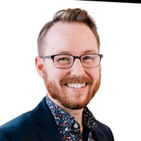
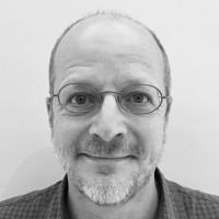
Kenneth Davis Email & Phone Number
Director Special Projects, VCSEL R and D
at
ams OSRAM
LinkedIn matched
✓ Verified Jul 2026
3 data sources
Profile completeness 86%
Current company
Role
Director Special Projects, VCSEL R and D
Location
Raleigh, North Carolina, United States
Company size
Who is Kenneth Davis? Overview
A concise factual answer block for searchers comparing this professional profile.
Quick answer
Kenneth Davis is listed as Director Special Projects, VCSEL R and D at ams OSRAM, a with 5161 employees, based in Raleigh, North Carolina, United States. AeroLeads shows a matched LinkedIn profile for Kenneth Davis.
Kenneth Davis previously worked as Director Special Projects, VCSEL R&D at Ams Osram and Head of Automotive LED Component Development at Cree Led. Kenneth Davis holds Doctor Of Philosophy - Phd, Materials Engineering from Rensselaer Polytechnic Institute.
Company email context
Email format at ams OSRAM
This section adds company-level context without repeating Kenneth Davis's masked contact details.
ams OSRAM
Review company-level records connected to Kenneth Davis before choosing the right outreach path.
Profile bio
About Kenneth Davis
My career continues to focus on the junction between R&D and manufacturing for the semiconductor and photonics industries. My skill and passion are to take concepts from the initial idea through R&D/NPI/qualification; inter- and intra-company technology transfer; industrialization; and manufacturing ramp. I have achieved development and manufacturing success through the management of multiple teams and programs via a combination of process and integration engineering problem solving in multiple cultural settings.Additional Experience:- Hirao Active Glass Project, ERATO, JRDC, Japan - Chief Researcher of Non-Linear Optic Materials- Osaka National Res. Inst., Osaka, Japan - AIST Fellowship/Visiting Scientist- Rensselaer Polytechnic Institute, Troy, NY - Research Assistant, Teaching Assistant & Instructor- Schott Glass Technologies, Duryea, PA - R&D Project Engineer & Assistant Batch House Foreman- Friedrich-Alexander University, Erlangen-Nuremburg, Germany - Laboratory Technician
Current workplace
Kenneth Davis's current company
Company context helps verify the profile and gives searchers a useful next step.
Ams Osram
8 roles
Kenneth Davis work experience
A career timeline built from the work history available for this profile.

Director Special Projects, Vcsel R&D
Director of Special Projects, VCSEL R&D, Princeton Optronics, Inc.- I was the lead interface between VCSEL R&D, customers, marketing, module development, and manufacturing.- Coordinator and author of RFI/RFQ responses and driver of sample deliveries for key customers and technologies.- I worked with our module and marketing teams to demonstrate viability and benefits of a new 1130nm VCSEL wavelength for behind OLED proximity modules with good performance and <1% screen distortion, in addition to other applications.CMP Lead for Planar Optics Development, Ang Mo Kio, Singapore (Special Project Request by Upper Management based on my IBM CMP Experience)- Drove grinding, lapping, and polishing process, pad, slurry, filtration, and carrier/jig design improvements to meet customer specifications for flatness, roughness, defectivity, bond-line recess with balanced polish removal for the opposite sides of a complex periscope optic.
Head Of Automotive Led Component Development
- I led a team of approximately 20 scientists and engineers to develop, qualify, and release into mass production LED-based automotive turn indicator, daylight running lights, and headlight modules. - Executed automotive NPI and reliability processes.- Transferred manufacturing and ongoing reliability testing capability to Cree’s factory in China. - Worked closely with manufacturing to ensure that all processes and controls were automotive ready to successfully pass the automotive customer audits. - Key developments included redevelopment of AuSn die attach metallurgy, resolution of panel corrosion and die attach issues, and development of a new TSV (surge protector) design and supplier.
Sep 2017 - Aug 2020

Director Of Led Die Development Integration
- I led a team of approximately 20 R&D engineers and scientists on InGaN and AlInGaP die development programs for Automotive, Flash, Illumination, and Display product platforms. - My team and I worked with design, process, EPI, and product development teams to ensure a strong product portfolio: improved thin film flip-chip blue/white LEDs to industry leading light output efficiency; increased high current reliability performance of chip-scale-package blue/white LED die to 350mA/mm2 for automotive applications; and improved red LED light output and reliability performance to competitive benchmarks.
Aug 2015 - Aug 2017
Senior Program Manager Of Ingan Led Die Development & Industrialization
- Co-developed and industrialized three generations of Lumiled’s first flip-chip CSP die for multiple generations of phone flash modules, UV LEDs, and Pixelated Headlights.- Ensured seamless integration of CSP processes into the Singapore wafer-fab and die-fab and ensured alignment with EPI R&D in San Jose; L1/L2 processes in Penang, Malaysia; and multiple vendors.
Jun 2011 - Jul 2015
45/32Nm Soi Npi And Technology Transfer Lead
- I revised IBM’s NPI methodology based on learning from the Chartered technology transfer project. - Educated and drove R&D and manufacturing teams to meet new NPI metrics for developing manufacturing-ready technologies for both 45 and 32nm technology nodes.- Led the technology transfer of 32nm SOI with high-K gates and embedded eDRAM to Global Foundries' teams in Malta, NY, USA and Dresden, Germany.
Aug 2007 - May 2011
Technology Transfer - Mol/Beol/Fbeol
- 300mm back-end and far back-end of line (BEOL & FBEOL) lead for 90nm technology transfer from IBM to Chartered Semiconductor the XBox 360 CPU.- Advised on tool selection and drove integration/process-output matching to help take Chartered Semiconductor (now Global Foundries) Fab 7 from a shell to qualification and manufacturing ramp. - Key contributor in diagnosing and solving challenging yield issues including a device clock issue.- Added middle-of-line (MOL) lead and front-end-of-line backup to BEOL responsibilities for 65nm.- Met every qualification, yield, and customer shipment target on time for both 90 and 65nm CPUs.
Jul 2004 - Jun 2007
Cmp & Insulator Deposition Manager & Process Engineer
Manager 300mm Cu CMP ----- Jul 2023 - Jun 2004- I led a taskforce and managed the process team to get 300mm Cu CMP back to 200mm capability and stability.Manager CMP & CVD/Spin-on Insulator Process Dev. Engineering ----- Jul 2001 – Jun 2003 - Managed CMP & insulator deposition process development teams (approximately 20 engineers).- Guided Poly-Si CMP & W CMP to similar process stability as Oxide, STI & Cu-CMP. - Led the insulator team through the difficult and high pressure down selection between spin-on and CVD-based low-k dielectric paths for IBM’s first low-k dielectric manufacturing release. Cu, Oxide, STI & Poly-Si CMP Process Development Engineer ----- Sep 1996 – Jun 2001- I started as the Oxide CMP lead and gradually worked on every process except for W-CMP.- Reduced scratching by 10x For STI & Oxide CMP.- Modified CMP carrier/jig design on outdated polishers to improve polish uniformity to match that of cutting-edge active-carrier polishers for a cost of less than $5k tool.- Worked with consumable manufacturers to incorporate the CMP carrier modifications into a consumable film to allow us to transfer the uniformity improvement to manufacturing fabs.- Took Cu CMP for IBM’s industry-leading interconnect BEOL from an unstable process (cleaning issues, pad variability, slurry particle instability, and immature understanding of the chemistry interactions with the process) to a stable, manufacturable process and transferred all learning to manufacturing.
Sep 1996 - Jun 2004
Team & coworkers
Colleagues at ams OSRAM
Other employees you can reach at osram.com. View company contacts for 5161 employees →
AS
 Ayu Setyaningrum
Colleague at Ams OsramPenang, Malaysia
View →
HN
Ayu Setyaningrum
Colleague at Ams OsramPenang, Malaysia
View →
HN
 Has Nina
Colleague at Ams OsramPenang, Malaysia
View →
JR
Has Nina
Colleague at Ams OsramPenang, Malaysia
View →
JR
 Julia Rothneichner
Colleague at Ams OsramRegensburg, Bavaria, Germany
View →
QS
Julia Rothneichner
Colleague at Ams OsramRegensburg, Bavaria, Germany
View →
QS
 Quan Shi
Colleague at Ams OsramWuxi, Jiangsu, China
View →
KA
Quan Shi
Colleague at Ams OsramWuxi, Jiangsu, China
View →
KA
 Kari Anne Lund
Colleague at Ams OsramOslo, Norway
View →
吕
Kari Anne Lund
Colleague at Ams OsramOslo, Norway
View →
吕
 吕汉钟
Colleague at Ams OsramFoshan, Guangdong, China
View →
MS
吕汉钟
Colleague at Ams OsramFoshan, Guangdong, China
View →
MS
 Markus Stauber
Colleague at Ams OsramRegensburg, Bavaria, Germany
View →
MI
Markus Stauber
Colleague at Ams OsramRegensburg, Bavaria, Germany
View →
MI
 Mahmod Ismail
Colleague at Ams OsramCairo, Egypt
View →
CX
Mahmod Ismail
Colleague at Ams OsramCairo, Egypt
View →
CX
 Cindy Xu
Colleague at Ams OsramBerkeley, California, United States
View →
RR
Cindy Xu
Colleague at Ams OsramBerkeley, California, United States
View →
RR
 Rajeev Ranjan
Colleague at Ams OsramDelhi, India
View →
Rajeev Ranjan
Colleague at Ams OsramDelhi, India
View →
Ayu Setyaningrum
Colleague at Ams OsramPenang, Malaysia
View →
HN
Has Nina
Colleague at Ams OsramPenang, Malaysia
View →
JR
Julia Rothneichner
Colleague at Ams OsramRegensburg, Bavaria, Germany
View →
QS
Quan Shi
Colleague at Ams OsramWuxi, Jiangsu, China
View →
KA
Kari Anne Lund
Colleague at Ams OsramOslo, Norway
View →
吕
吕汉钟
Colleague at Ams OsramFoshan, Guangdong, China
View →
MS
Markus Stauber
Colleague at Ams OsramRegensburg, Bavaria, Germany
View →
MI
Mahmod Ismail
Colleague at Ams OsramCairo, Egypt
View →
CX
Cindy Xu
Colleague at Ams OsramBerkeley, California, United States
View →
RR
Rajeev Ranjan
Colleague at Ams OsramDelhi, India
View →
2 education records
Kenneth Davis education
Doctor Of Philosophy - Phd, Materials Engineering

Bachelor'S Degree, Ceramic Sciences And Engineering
FAQ
Frequently asked questions about Kenneth Davis
Quick answers generated from the profile data available on this page.
What company does Kenneth Davis work for?
Kenneth Davis works for ams OSRAM.
What is Kenneth Davis's role at ams OSRAM?
Kenneth Davis is listed as Director Special Projects, VCSEL R and D at ams OSRAM.
Where is Kenneth Davis based?
Kenneth Davis is based in Raleigh, North Carolina, United States while working with ams OSRAM.
What companies has Kenneth Davis worked for?
Kenneth Davis has worked for Ams Osram, Cree Led, Lumileds, and Ibm.
Who are Kenneth Davis's colleagues at ams OSRAM?
Kenneth Davis's colleagues at ams OSRAM include Ayu Setyaningrum, Has Nina, Julia Rothneichner, Quan Shi, and Kari Anne Lund.
How can I contact Kenneth Davis?
You can use AeroLeads to view verified contact signals for Kenneth Davis at ams OSRAM, including work email, phone, and LinkedIn data when available.
What schools did Kenneth Davis attend?
Kenneth Davis holds Doctor Of Philosophy - Phd, Materials Engineering from Rensselaer Polytechnic Institute.
Find 750M verified contacts
Search by job title, company, industry, location, and seniority. Export verified B2B contact data when you need it.
Start free trialPeople with similar names
Check these profiles if this is not the Kenneth Davis you were looking for.
View similar profiles