
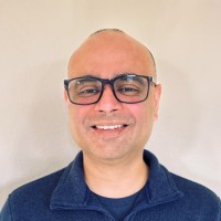
AeroLeads people directory · profile
Kuljit Virk Email & Phone Number
Principal Research Scientist
at
KLA
1 work email found
@kla-tencor.com
LinkedIn matched
✓ Verified July 2026
4 data sources
Profile completeness 100%
Who is Kuljit Virk? Overview
A concise factual answer block for searchers comparing this professional profile.
Quick answer
Kuljit Virk is listed as Principal Research Scientist at KLA, based in Fremont, California, United States. AeroLeads shows a work email signal at kla-tencor.com and a matched LinkedIn profile for Kuljit Virk.
Kuljit Virk previously worked as Senior Scientist Manager, Sensitivity Roadmap and Physics Modeling Group at Kla and Senior Research Scientist (Expert) at Kla. Kuljit Virk holds Ph.D, Physics, Semiconductors, Optics from University Of Toronto.
Company email context
Email format at KLA
This section adds company-level context without repeating Kuljit Virk's masked contact details.
{first}.{last}@kla-tencor.com
89% confidence
AeroLeads found 1 current-domain work email signal for Kuljit Virk. Compare company email patterns before reaching out.
Profile bio
About Kuljit Virk
Pioneering the physics behind tomorrow's semiconductor breakthroughs.Technical Leader and Physicist with 12 years of experience advancing R&D in the semiconductor industry, holding multiple patents in deep learning and optics. Pioneered novel theoretical and computational techniques as primary author of peer-reviewed works in ultrafast laser spectroscopy, open quantum systems, many-body physics, and optoelectronic devices. Expert in first principles-based approaches to the design of complex engineering systems. Actively pursuing research in quantum algorithms and quantum control of matter, impacting next-generation semiconductor technologies.My fascination with light-matter interactions has been the driving force behind my career. During my PhD and postdoc years, I explored exciton dynamics, decoherence, and energy transfer in photo-excited quantum wells and dots, building a strong foundation in first-principles modeling. For the past 12 years, I’ve applied this expertise in semiconductor R&D, tackling challenges like optoelectronic device simulation and anomaly detection. What excites me the most is turning complex problems into impactful technologies that push boundaries and create real-world value. A few highlights:• Developed accurate modeling of light scattering in patterned wafers, enabling a multitude of applications in wafer stack optimization and wafer inspection technology development.• Developed quantum device simulators for lasers and LEDs, securing industry contracts.• Invented an ultrafast optical + terahertz method to probe Berry phases in semiconductor quantum wells.Core competencies: * Density matrix and non-equilibrium Green's function approaches to model transport and decoherence in semiconductor systems. * Modeling of imaging systems, aberrations, wavefront shaping and structured illumination, and its application to develop engineering requirements for projection optics.* Modeling nonlinear optics phenomena and devices with classical and quantum states of light. * Electrodynamics in complex nanoscale media such as quantum dots, CMOS circuitry, and photonics devices. * Complete design and C++ implementation of ab-initio simulations of quantum well lasers, photodetectors, and electro-optic modulators.You may visit https://kuljitvirk.github.io/ to learn about some of the self-directed projects that I am currently working on.
Listed skills include Semiconductors, Physics, Optics, Matlab, and 31 others.
Current workplace
Kuljit Virk's current company
Company context helps verify the profile and gives searchers a useful next step.
8 roles
Kuljit Virk work experience
A career timeline built from the work history available for this profile.
Senior Scientist Manager, Sensitivity Roadmap And Physics Modeling Group
The scientific challenge in my work is to develop optical detection methods for CMOS device defects that are far below the diffraction limit at wavelengths yielding strong enough interaction to generate signals. My charter in BBP is to develop fundamental understanding of the sensitivity challenges in inspection as device technology evolves. Through in-depth modeling of optical scattering in upcoming devices, I and my team find potential solutions in both the optical and algorithm space and advise management in strategic technology development.I direct a team of PhD physicists that engages with advanced chipmakers in the early phase of each technology node and guides the optical inspection strategies based on the modeling and simulation paradigm I developed in the past 6 years. My team is also actively developing statistical learning-based anomaly detection technology that works by modeling the probability distribution of optical images of patterned wafers.Some published examples:Theoretical techniques that accelerate by 100X - 1000X the computation of scattering matrices of defects embedded in complex periodic media. Published in JOSAB 38, 1763 (2021)Ensemble of neural networks with false detection rate below 1 out of 100,000 while maintaining a true positive rate above 90%. This invention is based on the theory of weak learning. Patent Pending.
Senior Research Scientist (Expert)
• Developed and applied techniques for Monte-Carlo modeling of signal to noise ratio in all inspection layers for advanced logic, and new technologies such as gate all around devices.• Established a modeling paradigm within BBP by constructing an HPC ecosystem to aggregate large scale scattering simulations into probabilistic predictions of sensitivity.• Grew a deep multi-year modeling collaboration with Intel’s inspection R&D through technical engagements that demonstrated value of simulation to identify solutions and shorten time to results.• Invented deep neural net ensembles to achieve extremely low failure rate (less than 1E-5) defect detection in SEM images of patterned wafers, eliminating a key risk in the development of SEM review technology to process multi-million sites per hour.
Apr 2019 - Jun 2021
Senior Research Scientist (Staff)
Uncovered the fundamental limitations of signal-to-noise ratio in optical inspection of 3DNAND devices. This work played a key role in steering the company's technology development decisions for this market.
Apr 2017 - Mar 2019

Principal Engineer
In its Fremont facility, Western Digital produces wafers with magnetic read/write heads for hard disk drives. Everyday, the fab produces large amounts of metrology and process data as the wafers move through the manufacturing steps. My work at Western Digital was to create a physics-based data fusion system to predict writer head shapes and enable early detection of process excursions. The writer-head shape is critical to achieving high density storage.At the heart of the data-fusion system was a model that produced the surfaces 3D writer-heads as a function of parameters that could be discerned from analysis of metrology data. An automated analysis of CDSEM images extracted the head shape at the wafer surface, and combined that with metrology data from Ellipsometry, Atomic Force Microscopy, Focused Ion Beam Microscopy, to construct the full 3D writer shape below the wafer surface. I developed and integrated the system into the manufacturing line to create a quasi real-time prediction of the writer shapes over the entire wafer as it passed the key process steps.The new analysis methods and tools I developed for characterizing device variability led to process improvements and enabled detection of process excursions missed in standard metrology on test sites.
May 2015 - Apr 2017

Physicist, Device Simulation
At Silvaco, I was responsible for advancing its simulation capabilities in quantum electronics, quantum well lasers, photo-detectors, and passive photonic devices. I added to Silvaco's portfolio: * Ab-initio simulations of quantum well lasers with self-consistent band structure computation, electrostatic potentials, and charge density. * Modeling of distributed feedback lasers.* Simulators for organic light emitting diodes, with an effective model of Forster transfer between chromophores. * 2 dimensional Frequency Domain Finite Difference (FDFD) models along with Coupled Mode Theory to mode light propagation through structured waveguides, and electro-optic modulators. I also validated calculations based on analytical results where possible or corroboration with published literature. I prepared documentation of the implemented models and trained the application engineers for their use.
Oct 2012 - May 2015

Postdoctoral Research Scientist
• Developed and published an ab-intio (Density Functional Theory and Master Equations) approach to modeling nanostructures coupled to metallic surfaces, with applications to photovoltaics.• Created an exact and efficient method to calculate interfacial polarization in surface coupled nanocrystals, and identified novel charge transfer characteristics based on the approach.• Modeled quantum transport using NEGF in molecular junctions to analyze experimental data• Modeled terahertz light propagation and emission in layered semiconductors, and explained experimental data on radiation emitted by shift currents in quantum wells.
Apr 2010 - Oct 2012

Doctoral Research
• Developed a Keldysh Green functions formalism to derive non-linear optical susceptibility and ultrafast spectroscopy of many body systems. • Invented an ultrafast optical technique to probe Berry phases in semiconductors.• Performed an early study of the decoherence of qubits in Si:P system due to conduction electrons.• Developed a new approach to compute high-field excitation of semiconductors in length gauge based on the concept of Wilson loops in lattice gauge theory. • Primary author of 6 peer-reviewed journal articles and presented at international conferences
Sep 2004 - Dec 2009
Team & coworkers
Colleagues at KLA
Other employees you can reach at kla-tencor.com. View company contacts →
LF
 Leanne Farmer
Colleague at KlaSan Francisco Bay Area, United States
View →
PK
Leanne Farmer
Colleague at KlaSan Francisco Bay Area, United States
View →
PK
 Prathik Kulkarni
Colleague at KlaSan Francisco Bay Area, United States
View →
TP
Prathik Kulkarni
Colleague at KlaSan Francisco Bay Area, United States
View →
TP
 Tomas P.
Colleague at KlaAnn Arbor, Michigan, United States
View →
SB
Tomas P.
Colleague at KlaAnn Arbor, Michigan, United States
View →
SB
 Steve Biellak
Colleague at KlaMilpitas, California, United States
View →
MH
Steve Biellak
Colleague at KlaMilpitas, California, United States
View →
MH
 Marc Harwin
Colleague at KlaUnited States
View →
RT
Marc Harwin
Colleague at KlaUnited States
View →
RT
 Rodney Torii
Colleague at KlaSan Francisco Bay Area, United States
View →
CT
Rodney Torii
Colleague at KlaSan Francisco Bay Area, United States
View →
CT
 Carie Torrence
Colleague at KlaAnn Arbor, Michigan, United States
View →
DA
Carie Torrence
Colleague at KlaAnn Arbor, Michigan, United States
View →
DA
 Derek Ashburn
Colleague at KlaPlymouth, Michigan, United States
View →
CY
Derek Ashburn
Colleague at KlaPlymouth, Michigan, United States
View →
CY
 Christie Yu, Ctp
Colleague at KlaMilpitas, California, United States
View →
JR
Christie Yu, Ctp
Colleague at KlaMilpitas, California, United States
View →
JR
 Jagan Raj Raviraja
Colleague at KlaTamil Nadu, India
View →
Jagan Raj Raviraja
Colleague at KlaTamil Nadu, India
View →
Leanne Farmer
Colleague at KlaSan Francisco Bay Area, United States
View →
PK
Prathik Kulkarni
Colleague at KlaSan Francisco Bay Area, United States
View →
TP
Tomas P.
Colleague at KlaAnn Arbor, Michigan, United States
View →
SB
Steve Biellak
Colleague at KlaMilpitas, California, United States
View →
MH
Marc Harwin
Colleague at KlaUnited States
View →
RT
Rodney Torii
Colleague at KlaSan Francisco Bay Area, United States
View →
CT
Carie Torrence
Colleague at KlaAnn Arbor, Michigan, United States
View →
DA
Derek Ashburn
Colleague at KlaPlymouth, Michigan, United States
View →
CY
Christie Yu, Ctp
Colleague at KlaMilpitas, California, United States
View →
JR
Jagan Raj Raviraja
Colleague at KlaTamil Nadu, India
View →
3 education records
Kuljit Virk education
Ph.D, Physics, Semiconductors, Optics
University Of Toronto
Master Of Science, Physics, Semiconductors, Optics
University Of Toronto
Basc, Engineering Physics
The University Of British Columbia
FAQ
Frequently asked questions about Kuljit Virk
Quick answers generated from the profile data available on this page.
What company does Kuljit Virk work for?
Kuljit Virk works for KLA.
What is Kuljit Virk's role at KLA?
Kuljit Virk is listed as Principal Research Scientist at KLA.
What is Kuljit Virk's email address?
AeroLeads has found 1 work email signal at @kla-tencor.com for Kuljit Virk at KLA.
Where is Kuljit Virk based?
Kuljit Virk is based in Fremont, California, United States while working with KLA.
What companies has Kuljit Virk worked for?
Kuljit Virk has worked for Kla, Wd, A Western Digital Company, Silvaco, Columbia University, and University Of Toronto.
Who are Kuljit Virk's colleagues at KLA?
Kuljit Virk's colleagues at KLA include Leanne Farmer, Prathik Kulkarni, Tomas P., Steve Biellak, and Marc Harwin.
How can I contact Kuljit Virk?
You can use AeroLeads to view verified contact signals for Kuljit Virk at KLA, including work email, phone, and LinkedIn data when available.
What schools did Kuljit Virk attend?
Kuljit Virk holds Ph.D, Physics, Semiconductors, Optics from University Of Toronto.
What skills is Kuljit Virk known for?
Kuljit Virk is listed with skills including Semiconductors, Physics, Optics, Matlab, Simulations, Materials Science, Computational Physics, and Quantum Theory.
Find 750M verified contacts
Search by job title, company, industry, location, and seniority. Export verified B2B contact data when you need it.
Start free trial