
Principal Digital Design Engineer
Current
Jul 2020 - Present
Please complete the CAPTCHA to continue
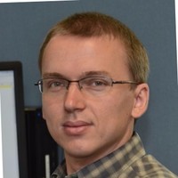
A concise factual answer block for searchers comparing this professional profile.
Leoš Kafka is listed as Principal Digital Design Engineer at Dialog Semiconductor, a with 1790 employees, based in Prague, Czechia, Czech Republic. AeroLeads shows a matched LinkedIn profile for Leoš Kafka.
Leoš Kafka previously worked as Staff IC Design Engineer at Adesto Technologies and Staff IC Design Engineer at S3 Group. Leoš Kafka holds Ph.D., Information Science And Computer Engineering from České Vysoké Učení Technické V Praze.
This section adds company-level context without repeating Leoš Kafka's masked contact details.
Review company-level records connected to Leoš Kafka before choosing the right outreach path.
Ten year’s experience in digital circuit design and verificationProfessional Skills:• Digital design languages: VHDL, Verilog• Digital design tools: Xilinx ISE and XPS, Synopsis Synplify• Verification languages: VHDL, SystemVerilog• Verification tools: Mentor Graphics ModelSim and Questa• Design flow control script languages: BASH, Perl• Embedded processor architectures: Gaisler LEON3, Xilinx MicroBlaze• Bus architectures: AMBA AHB and AXI, IBM CoreConnect • External interfaces: PCI, Ethernet, SPI, I2C• Programmable devices: Xilinx FPGAs and CPLDs• Microcontrollers: Atmel AVR
Listed skills include Vhdl, Rtl Design, Fpga, Xilinx, and 14 others.
Company context helps verify the profile and gives searchers a useful next step.
A career timeline built from the work history available for this profile.



Hlavní Město Praha, Česká Republika
Responsibilities:• Preparation of product documentation according to customer requirements• Design and implementation of PLDs for prototypes and final products• Verification through simulation and in-lab tests (US)

Hlavní Město Praha, Česká Republika
Participating in national (2) and European (4) projects:• SMECY – development of an embedded system for video-applications• Apple-CORE – implementation of the micro-thread UTLEON3 processor• RETAC – development of a platform for fault emulation through FPGAs• RECONF2 – development of tools for partial runtime reconfiguration of FPGAsResponsibilities:• Architecture exploration• Documentation through project reports and conference papers• Design and verification in VHDL• Development of support tools in BASH and Perl

Leuven, Belgium
Participating in a project dealing with SoC circuits for multimediaResponsibilities:• Preparation of specification• Development of models in SystemC• Design and verification in VHDL
Other employees you can reach at dialog-semiconductor.com. View company contacts for 1790 employees →
 Eunju Lee
Colleague at Dialog SemiconductorSouth Korea, Korea, Republic Of
View →
EC
Eunju Lee
Colleague at Dialog SemiconductorSouth Korea, Korea, Republic Of
View →
EC
 Erwin Cordero
Colleague at Dialog SemiconductorTaichung City, Taiwan, Province Of China
View →
CW
Erwin Cordero
Colleague at Dialog SemiconductorTaichung City, Taiwan, Province Of China
View →
CW
 Cliff Wang
Colleague at Dialog SemiconductorTaiwan, Province Of China
View →
MP
Cliff Wang
Colleague at Dialog SemiconductorTaiwan, Province Of China
View →
MP
 Madhu P S
Colleague at Dialog SemiconductorChandler, Arizona, United States
View →
RH
Madhu P S
Colleague at Dialog SemiconductorChandler, Arizona, United States
View →
RH
 Ruei Hong Peng
Colleague at Dialog SemiconductorHsinchu City, Taiwan, Province Of China
View →
AM
Ruei Hong Peng
Colleague at Dialog SemiconductorHsinchu City, Taiwan, Province Of China
View →
AM
 Ameya Mahadik
Colleague at Dialog SemiconductorUnited States
View →
RA
Ameya Mahadik
Colleague at Dialog SemiconductorUnited States
View →
RA
 Raff Achour
Colleague at Dialog SemiconductorGreater Reading Area, United Kingdom
View →
DD
Raff Achour
Colleague at Dialog SemiconductorGreater Reading Area, United Kingdom
View →
DD
 Doug Daley
Colleague at Dialog SemiconductorIdaho Falls, Idaho, United States
View →
JK
Doug Daley
Colleague at Dialog SemiconductorIdaho Falls, Idaho, United States
View →
JK
 Jon Kurtz
Colleague at Dialog SemiconductorPittsburgh, Pennsylvania, United States
View →
AS
Jon Kurtz
Colleague at Dialog SemiconductorPittsburgh, Pennsylvania, United States
View →
AS
 Alice Shao
Colleague at Dialog SemiconductorShenzhen, Guangdong, China
View →
Alice Shao
Colleague at Dialog SemiconductorShenzhen, Guangdong, China
View →

Czech Technical University in Prague, Faculty of Electrical Engineering Doctoral thesis: Fault Emulation Techniques for Generic Netlists.
Czech Technical University in Prague, Faculty of Electrical Engineering Diploma work: Design of Fault Tolerant Circuits in FPGAs
Quick answers generated from the profile data available on this page.
Leoš Kafka works for Dialog Semiconductor.
Leoš Kafka is listed as Principal Digital Design Engineer at Dialog Semiconductor.
Leoš Kafka is based in Prague, Czechia, Czech Republic while working with Dialog Semiconductor.
Leoš Kafka has worked for Dialog Semiconductor, Adesto Technologies, S3 Group, Honeywell Aerospace, and Institute Of Information Theory And Automation Of The Ascr.
Leoš Kafka's colleagues at Dialog Semiconductor include Eunju Lee, Erwin Cordero, Cliff Wang, Madhu P S, and Ruei Hong Peng.
You can use AeroLeads to view verified contact signals for Leoš Kafka at Dialog Semiconductor, including work email, phone, and LinkedIn data when available.
Leoš Kafka holds Ph.D., Information Science And Computer Engineering from České Vysoké Učení Technické V Praze.
Leoš Kafka is listed with skills including Vhdl, Rtl Design, Fpga, Xilinx, Linux, Bash, Digital Circuit Design, and Programming.
Search by job title, company, industry, location, and seniority. Export verified B2B contact data when you need it.
Start free trial Search contacts