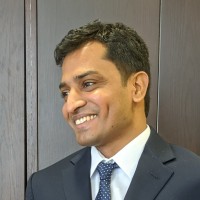
Mahender Kumar
AeroLeads people directory · profile

Mahender Kumar Email & Phone Number

Principal Member of Technical Staff (Foundry Technology Interface) at Avera Semiconductor at Avera Semiconductor
Location: Santa Clara, California, United States 7 work roles 3 schools
1 work email found @globalfoundries.com 2 phones found area 408 LinkedIn matched
✓ Verified May 2026 4 data sources Profile completeness 100%

Contact Signals · 1 work email · 2 phones

Work email m****@globalfoundries.com
Direct phone (408) ***-****
LinkedIn Profile matched
3 free lookups remaining · No credit card
Current company
Avera Semiconductor
Role
Principal Member of Technical Staff (Foundry Technology Interface) at Avera Semiconductor
Location
Santa Clara, California, United States

Who is Mahender Kumar? Overview

A concise factual answer block for searchers comparing this professional profile.

Quick answer

Mahender Kumar is listed as Principal Member of Technical Staff (Foundry Technology Interface) at Avera Semiconductor at Avera Semiconductor, based in Santa Clara, California, United States. AeroLeads shows a work email signal at globalfoundries.com, phone signal with area code 408, and a matched LinkedIn profile for Mahender Kumar.

Mahender Kumar previously worked as Principal Member of Technical Staff (Foundry Technology Interface) at Avera Semiconductor and Principal Member of Technical Staff (Design Technology Co-Optimization (DTCO)) at Globalfoundries. Mahender Kumar holds Doctor Of Philosophy (Ph.D.), Electrical And Electronics Engineering from The Hong Kong University Of Science And Technology.

Company email context

Email format at Avera Semiconductor

This section adds company-level context without repeating Mahender Kumar's masked contact details.

{first}.{last}@globalfoundries.com
86% confidence

AeroLeads found 1 current-domain work email signal for Mahender Kumar. Compare company email patterns before reaching out.

Profile bio

About Mahender Kumar

Over 20 years of experience in silicon technology and hardware product development, process integration and device architectures, process specifications and design rules development for PDKs, design technology co-optimization (DTCO), foundry interface, process and product design interactions (DFx), design of experiments (DOE), test structure design for process and product yield and reliability learning, excellent cross-functional teams leadership and communications skills, over 30 publications & 31 filed/issued patents.

Listed skills include Cmos, Design Of Experiments, Semiconductors, Characterization, and 22 others.

Current workplace

Mahender Kumar's current company

Company context helps verify the profile and gives searchers a useful next step.

Avera Semiconductor
Avera Semiconductor
Principal Member of Technical Staff (Foundry Technology Interface) at Avera Semiconductor
7 roles

Mahender Kumar work experience

A career timeline built from the work history available for this profile.

Principal Member Of Technical Staff (Foundry Technology Interface)

Current
Avera Semiconductor

Santa Clara California

Foundry interface technologist for 7nm and 5nm CMOS technology nodes for AveraSemi ASIC product design teams. Managed and delivered closure of device, technology, reliability, and PDK issues on a very tight schedule to meet ASIC hardware product design performance, power, yield, and reliability requirements. Created a special wafer acceptance test (WAT).

Oct 2018 - Present

Principal Member Of Technical Staff (Design Technology Co-Optimization (Dtco))

Santa Clara, California And Malta, New York

Leading-edge 7nm and 5nm semiconductor CMOS technology definition: process flow and device architectures, process specifications for fab and PEX /device models, design rules, standard cells and SRAM memory bit cell definition to meet hardware design performance, power, yield, and reliability requirements.Semiconductor process integration and device.

Jul 2015 - Oct 2018

Senior Engineer (Process Integration And Yield) Ibm Assignee To Globalfoundries

Ibm

Malta, New York

Improved 20nm semiconductor CMOS technology for product development and manufacturing compliance of process specifications, design rule with product performance, power, yield, and lifecycle reliability requirements by working together with technology development and manufacturing organizations.

Jun 2014 - Jun 2015

Senior Engineer (Process Integration And Yield)

Ibm

East Fishkill, New York

Played a senior technical leadership role in definition, development, and manufacturing of 65nm, 32nm and 22nm semiconductor silicon-on-insulator (SOI) CMOS technologies for IBM server system product as well as for ASIC product on a very aggressive schedule.Semiconductor process technology representative to work with IBM server and ASIC product design.

Oct 2003 - May 2014

Advisory Engineer (Process Integration And Yield)

Ibm

East Fishkill, New York

Demonstrated the feasibility of semiconductor SOI embedded DRAM (eDRAM) in 90nm SOI CMOS process technology. Which has been used in IBM server product starting from semiconductor SOI CMOS 45nm technology node. This innovation and vision has high impact on system performance for IBM SOI CMOS technology and server hardware product.Semiconductor process.

Sep 2001 - Oct 2003

Research Associate

New Delhi, India

Demonstrated integrated photonics optical splinter/divider feasibility and worked on MEMS cantilevers.

Mar 1996 - Aug 1997

Junior Research Fellow (Jrf)

Ahmedabad, Gujrat, India

Collected data for a remote-sensing satellite camera calibration. Calibration of camera improved the data quality, this satellite data created market opportunities for ISRO India to sell to other countries. It created international market for ISRO >10M.

Sep 1995 - Mar 1996
3 education records

Mahender Kumar education

Master'S Degree, Electronics

Activities and Societies: Cultural activities.Device and technology.

FAQ

Frequently asked questions about Mahender Kumar

Quick answers generated from the profile data available on this page.

What company does Mahender Kumar work for?

Mahender Kumar works for Avera Semiconductor.

What is Mahender Kumar's role at Avera Semiconductor?

Mahender Kumar is listed as Principal Member of Technical Staff (Foundry Technology Interface) at Avera Semiconductor at Avera Semiconductor.

What is Mahender Kumar's email address?

AeroLeads has found 1 work email signal at @globalfoundries.com for Mahender Kumar at Avera Semiconductor.

What is Mahender Kumar's phone number?

AeroLeads has found 2 phone signal(s) with area code 408 for Mahender Kumar at Avera Semiconductor.

Where is Mahender Kumar based?

Mahender Kumar is based in Santa Clara, California, United States while working with Avera Semiconductor.

What companies has Mahender Kumar worked for?

Mahender Kumar has worked for Avera Semiconductor, Globalfoundries, Ibm, Indian Institute Of Technology, Delhi, and Indian Space Research Organisation (Isro).

How can I contact Mahender Kumar?

You can use AeroLeads to view verified contact signals for Mahender Kumar at Avera Semiconductor, including work email, phone, and LinkedIn data when available.

What schools did Mahender Kumar attend?

Mahender Kumar holds Doctor Of Philosophy (Ph.D.), Electrical And Electronics Engineering from The Hong Kong University Of Science And Technology.

What skills is Mahender Kumar known for?

Mahender Kumar is listed with skills including Cmos, Design Of Experiments, Semiconductors, Characterization, Ic, Process Integration, Asic, and Testing.

Find 750M verified contacts

Search by job title, company, industry, location, and seniority. Export verified B2B contact data when you need it.

People with similar names

Check these profiles if this is not the Mahender Kumar you were looking for.

View similar profiles