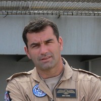
Senior Scientist
CurrentR&D projects related to High-Reliability Electronics in Harsh Environments (Radiation, Extreme Temperatures, Space Electronics)
Jan 2019 - Present
Please complete the CAPTCHA to continue
@alphacoreinc.com
✓
4 phones found area 256 and 408
✓
LinkedIn matched
A concise factual answer block for searchers comparing this professional profile.
Marek Turowski is listed as Senior Scientist at Alphacore Inc. at Alphacore Inc., a company with 28 employees, based in Greater Phoenix Area, United States, United States. AeroLeads shows a work email signal at alphacoreinc.com, phone signal with area code 256, 408, and a matched LinkedIn profile for Marek Turowski.
Marek Turowski previously worked as Senior Scientist at Alphacore Inc. and Senior TCAD Applications Engineer at Silvaco Inc. Marek Turowski holds Doctor Of Philosophy - Phd, Electronics Engineering from Technical University Of Lodz.
This section adds company-level context without repeating Marek Turowski's masked contact details.
AeroLeads found 1 current-domain work email signal for Marek Turowski. Compare company email patterns before reaching out.
* In-depth knowledge and understanding of semiconductor device physics of a broad range of semiconductor technologies, including CMOS, Bipolar, BiCMOS, high-voltage and power devices, FinFETs, SOI, SiGe, III-V, HBTs, HEMTs. * Over 25 years of experience in modeling, simulation, and multi-domain (electrical, thermal, and optical) analysis, optimization, and characterization of semiconductor devices and ICs: Si, SiGe, III-V, power devices, optoelectronic/photonic and high-frequency/RF devices.* Radiation effects in semiconductor devices and ICs: single-event effects (SEEs), single-event upsets, soft errors, total ionizing dose (TID), and displacement damage (DD). Deep knowledge of radiation effects on all levels, from detailed physics to devices to circuits to soft error rates (SER). * Over 15 years of demonstrated technical leadership and project management experience.* Knowledge of integrated circuit (IC) fabrication process, reliability issues and physics.* Over 15 years of extensive hands-on experience with TCAD Process and Device simulation tools.* Familiar with Layout tools, DRC, LVS, and parasitics extraction.* Circuit simulation tools (Spice, and similar); knowledge of many Spice/compact models.* Co-author of over 200 technical papers.Publications: http://scholar.google.com/citations?user=nsJqhZsAAAAJ&hl=enSpecialties: Physics of semiconductor devices, reliability, modeling, simulation, TCAD, radiation effects, thermal issues, extreme environments
Listed skills include Simulations, Semiconductors, Physics, Ic, and 21 others.
Company context helps verify the profile and gives searchers a useful next step.
A career timeline built from the work history available for this profile.
Phoenix Metropolitan Area, Arizona, United States
R&D projects related to High-Reliability Electronics in Harsh Environments (Radiation, Extreme Temperatures, Space Electronics)

San Francisco Bay Area
Semiconductor Devices and Processes - Physics Based Modeling, Simulation, Design, Optimization

Pleasanton, California, United States
TCAD and Mixed-Mode tools and simulations of a wide range of semiconductor technologies, devices and circuits, including: 180nm...14nm CMOS, bulk, SOI, FinFETs, SiGe, HBT, III-V, HEMTs, SRAM, DRAM, etc. Studies and mitigation of radiation effects in semiconductor devices and ICs, especially single-event effects (SEEs) and soft errors. Enhanced expertise of.

Huntsville, Alabama, United States
Led many R&D projects involving modeling, simulation, analysis, and computer-aided-design of semiconductor devices (TCAD), integrated circuits, photonic & optoelectronic devices, MEMS, RF ICs, heating/cooling of semiconductor chips and packages, electromagnetics, space radiation effects, extreme environments.

EE Dept: Research on new methods of modeling of semiconductor devices
Electronics Engineering, VLSI, IC Design, CAD
Sydney, New South Wales, Australia
Modeling of Electromagnetic Fields
Other employees you can reach at alphacoreinc.com. View company contacts for 28 employees →
 Adalin Benedetto
Colleague at Alphacore Inc.Tempe, Arizona, United States, United States
View →
JP
Adalin Benedetto
Colleague at Alphacore Inc.Tempe, Arizona, United States, United States
View →
JP
 Jyrki Penttinen
Colleague at Alphacore Inc.Phoenix, Arizona, United States, United States
View →
DM
Jyrki Penttinen
Colleague at Alphacore Inc.Phoenix, Arizona, United States, United States
View →
DM
 Debnath Maiti
Colleague at Alphacore Inc.Tempe, Arizona, United States, United States
View →
SO
Debnath Maiti
Colleague at Alphacore Inc.Tempe, Arizona, United States, United States
View →
SO
 Sein Oh
Colleague at Alphacore Inc.South Korea, Korea, Republic Of
View →
YC
Sein Oh
Colleague at Alphacore Inc.South Korea, Korea, Republic Of
View →
YC
 Yuan Chao
Colleague at Alphacore Inc.San Jose, California, United States, United States
View →
SC
Yuan Chao
Colleague at Alphacore Inc.San Jose, California, United States, United States
View →
SC
 Sai Chetana Kunapareddy
Colleague at Alphacore Inc.Tempe, Arizona, United States, United States
View →
DS
Sai Chetana Kunapareddy
Colleague at Alphacore Inc.Tempe, Arizona, United States, United States
View →
DS
 Dr Shantanu Mehta
Colleague at Alphacore Inc.India, India
View →
AN
Dr Shantanu Mehta
Colleague at Alphacore Inc.India, India
View →
AN
 Alfredo Nevarez
Colleague at Alphacore Inc.Buda, Texas, United States, United States
View →
AH
Alfredo Nevarez
Colleague at Alphacore Inc.Buda, Texas, United States, United States
View →
AH
 Alphacore Hiring
Colleague at Alphacore Inc.Greater Phoenix Area, United States
View →
JR
Alphacore Hiring
Colleague at Alphacore Inc.Greater Phoenix Area, United States
View →
JR
 Jeevana Reddy
Colleague at Alphacore Inc.Tempe, Arizona, United States, United States
View →
Jeevana Reddy
Colleague at Alphacore Inc.Tempe, Arizona, United States, United States
View →

Quick answers generated from the profile data available on this page.
Marek Turowski works for Alphacore Inc..
Marek Turowski is listed as Senior Scientist at Alphacore Inc. at Alphacore Inc..
AeroLeads has found 1 work email signal at @alphacoreinc.com for Marek Turowski at Alphacore Inc..
AeroLeads has found 4 phone signal(s) with area code 256, 408 for Marek Turowski at Alphacore Inc..
Marek Turowski is based in Greater Phoenix Area, United States, United States while working with Alphacore Inc..
Marek Turowski has worked for Alphacore Inc., Silvaco Inc, Robust Chip Inc., Cfd Research Corporation, and University Of Kentucky.
Marek Turowski's colleagues at Alphacore Inc. include Adalin Benedetto, Jyrki Penttinen, Debnath Maiti, Sein Oh, and Yuan Chao.
You can use AeroLeads to view verified contact signals for Marek Turowski at Alphacore Inc., including work email, phone, and LinkedIn data when available.
Marek Turowski holds Doctor Of Philosophy - Phd, Electronics Engineering from Technical University Of Lodz.
Marek Turowski is listed with skills including Simulations, Semiconductors, Physics, Ic, R&D, Electronics, Modeling, and Vlsi.
Search by job title, company, industry, location, and seniority. Export verified B2B contact data when you need it.
Start free trial Search contactsCheck these profiles if this is not the Marek Turowski you were looking for.
View similar profiles