
AeroLeads people directory · profile
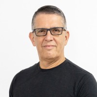
Mario Faria Email & Phone Number
Americas Semiconductor and Coating Segment Director
at
INFICON
1 work email found
@maxieg.com
1 phone found area 214
LinkedIn matched
✓ Verified July 2026
4 data sources
Profile completeness 100%
Current company
Role
Americas Semiconductor and Coating Segment Director
Location
Greater Tampa Bay Area, United States
Company size
Who is Mario Faria? Overview
A concise factual answer block for searchers comparing this professional profile.
Quick answer
Mario Faria is listed as Americas Semiconductor and Coating Segment Director at INFICON, a with 1093 employees, based in Greater Tampa Bay Area, United States. AeroLeads shows a work email signal at maxieg.com, phone signal with area code 214, and a matched LinkedIn profile for Mario Faria.
Mario Faria previously worked as Director Semiconductor Solutions at Tignis and Partner & Vice President Operations at The Max Group - Max I.E.G. Llc. Mario Faria holds Executive Mba, Business Administration, Management And Operations from University Of Florida - Warrington College Of Business.
Company email context
Email format at INFICON
This section adds company-level context without repeating Mario Faria's masked contact details.
{first}_{last}@maxieg.com
86% confidence
AeroLeads found 1 current-domain work email signal for Mario Faria. Compare company email patterns before reaching out.
Profile bio
About Mario Faria
Results driven dynamic leader with 24 years of progressive leadership in Semiconductors production optimization and delivery of improvement solutions . Broad technical background with in-depth understanding of product development and manufacturing processes. Effectively balance big picture with innovative thinking, resource efficiency, cost savings and strategic execution. Successfully managed products from design to production, optimized production strategy to maximize profits and implemented solutions to improve OEE, yield and overall output. Strength in managing cross-functional teams; easily establish and maintain positive working relationships. Thrive in diverse and international environments. Outstanding analytical skills, AI/ML solutions, Lean Six-Sigma certified, Project Management experience, and effective leader.Specialties: Analytical skills, Operational Efficiency, Program Management, NPI, Process Optimization, Test and Qualification, Service & Software Solutions Sales and Marketing experience. Knowledge in data analytics, AI/ML, Lean Six-Sigma, leadership skills, process engineering, profit enhancement, project management, global workforce, sees the big picture, thrives in challenging environments, MS office expert.
Listed skills include Semiconductors, Ic, Manufacturing, Program Management, and 46 others.
Current workplace
Mario Faria's current company
Company context helps verify the profile and gives searchers a useful next step.
Inficon
9 roles
Mario Faria work experience
A career timeline built from the work history available for this profile.

Director Semiconductor Solutions
CurrentDefining and delivering Artificial Intelligence and Machine Learning solutions for Semiconductors OEMs and Wafer Fabs. Serve as the central function and driving force for the design, strategy, marketing, and business development for Tignis’ products in the semiconductor market.
Jul 2022 - Present
Partner & Vice President Operations
Responsible for segment growth providing operational improvement products and services, NPI best known practices and smart manufacturing solutions. Lead business development activities and ownership of client management for execution of new and sustaining projects. Full P&L accountability for Americas market, hiring and team development. Main point of contact to customer and management of MAX team at customer’s site.
Jan 2015 - Jul 2022
Project Manager Consultant
Senior Consultant providing unique range of operational solutions focusing on product development cycle time reduction, project management effectiveness, and overall business process improvement in the semiconductor and compound semiconductors industries.LED product development experience supporting LED industry leader NPD & R&D organization in time-to-market acceleration, organization transformation, re-definition of phase gated process, R&D Supply Chain planning & execution process… Show more Senior Consultant providing unique range of operational solutions focusing on product development cycle time reduction, project management effectiveness, and overall business process improvement in the semiconductor and compound semiconductors industries.LED product development experience supporting LED industry leader NPD & R&D organization in time-to-market acceleration, organization transformation, re-definition of phase gated process, R&D Supply Chain planning & execution process, and improving overall program management techniques.PM for Solar module project to improve their OEE by 40%. Focus on analyzing labor resource between tools and workstations to maximize attendance at bottlenecks, redesign ways of working, material flows (eg line versus cluster), WIP staging points, increase starts levels, and remove any constraints preventing the factory from ramping quickly. Currently PM for major LED manufacturer in Malaysia providing a study in productivity improvements for one of the high volume runner products and one of the new innovative product lines on the back-end assembly processes. Show less
Dec 2010 - Dec 2014
Product/Project Engineer
Project engineering responsibilities including planning, scheduling, vendor contractor selection, and resource allocation for project with program management teamHeavy interaction with ASIC design team to have design for test and design for manufacturability guidelines in place on new designsTechnical project management tasks including parts selection and procurement, system in package and multi-chip module design interaction, design package control management documentation ownership… Show more Project engineering responsibilities including planning, scheduling, vendor contractor selection, and resource allocation for project with program management teamHeavy interaction with ASIC design team to have design for test and design for manufacturability guidelines in place on new designsTechnical project management tasks including parts selection and procurement, system in package and multi-chip module design interaction, design package control management documentation ownership, functional test analysis.ASIC product engineering responsibilities include planning, scheduling, cost, vendor contractor selection, product prototype to production flow definitions, test spec and qualification plans.ASIC foundries technical understanding of digital and RF process specs to be able to pick right technology for desired customer application needs.Maintain vendor relationship and continue researching and making sure vendors maintain ITAR compliance and other required documentation to be an approved vendor to ITT.Assure of best achievable product profit margins by test time reduction, lower cost test (ATE) solution and vendor sub-contractor negotiated costs. Show less
Oct 2007 - Nov 2010

Lead Product Engineer
Managed technical activities for team of 6 product engineers and 8 projectsReported to senior management and customers project status and achievementsCo-developed standardize procedures for best practices in design for test (DFT) Weekly interaction with manufacturing facility in the Philippines, monitor yield reports, suggested process improvementsAssisted junior engineers in professional development; reviewed and schedule tasks to improve skill sets, identified… Show more Managed technical activities for team of 6 product engineers and 8 projectsReported to senior management and customers project status and achievementsCo-developed standardize procedures for best practices in design for test (DFT) Weekly interaction with manufacturing facility in the Philippines, monitor yield reports, suggested process improvementsAssisted junior engineers in professional development; reviewed and schedule tasks to improve skill sets, identified strengths/weaknesses and communicated with section managerRepresented ASIC product development team during vendor's technical meetings, roadmap reviews, and external industry's conference on IC design and test Show less
Aug 2006 - Oct 2007
Product Development Engineer
Texas Instruments, Inc
Highly integrated devices with short time cycles to release to production, fast pace environment with ability to multitask across different devicesHardware/Software development of new ASIC devices with complete engineering characterization analysis of initial siliconProcess characterization, qualification, release to production, ramp-to-volumeWork closely with fabs/design team to quickly resolve yield issues observed on ATE side - some exposure to fab and simulation data for… Show more Highly integrated devices with short time cycles to release to production, fast pace environment with ability to multitask across different devicesHardware/Software development of new ASIC devices with complete engineering characterization analysis of initial siliconProcess characterization, qualification, release to production, ramp-to-volumeWork closely with fabs/design team to quickly resolve yield issues observed on ATE side - some exposure to fab and simulation data for designsProduction release offloads with multiple overseas trips to ensure quality handoffs to production sites, work cross functional with engineering teams Part of profit enhancement team - concentrate on improving device cost of business margins, contributing to bottom line PFO for business groupDevice optimizations to test times, burn-in reduction, yield improvements and/or ATE platform conversions for less expensive test costCollect and analyze data and reliability stress data to identify gaps in design performance, quality and reliability. Identification and implementation of containment and corrective actions to resolve gapsWork closely with external customer and quality engineering on field returns to ensure right test coverage in place in production release programs Show less
Oct 2004 - Aug 2006

Applications Engineer
Product engineer support for ASIC group at customer, Texas Instruments. Responsible for device development from hardware design/test program development to analysis, yield tracking and solving test related issuesLTX Fusion HF semiconductor tester applications support for Sparc architecture technologies at customer site, Texas Instruments.Custom test code development for different applications in memory groups for SRAM testing.Memory custom test methods development and support using… Show more Product engineer support for ASIC group at customer, Texas Instruments. Responsible for device development from hardware design/test program development to analysis, yield tracking and solving test related issuesLTX Fusion HF semiconductor tester applications support for Sparc architecture technologies at customer site, Texas Instruments.Custom test code development for different applications in memory groups for SRAM testing.Memory custom test methods development and support using e-fuse repair and Die ID on Sun 90nm device.White paper description for e-fuse programming methodology using LTX Fusion Platform.Full support for production and engineering groups for any tester malfunction, hardware or software related.Performance Evaluation between LTX VX250/VX4 Fusion testers on Sparc Device Show less
Jun 2002 - Oct 2004
Test/Characterization Engineer
Ibm Microelectronics
Synchronous DRAM design verification for .14um technology: Full product development involvement including initial hardware test and characterization of different process split lots, analyzing data and characterizing tests to minimize yield lost, recommended different voltage/timing parameters to design team for manufacturing team based on results collected, optimization for best post-fused wafers and package level test programs. Development and maintenance of ATE code (Teradyne &… Show more Synchronous DRAM design verification for .14um technology: Full product development involvement including initial hardware test and characterization of different process split lots, analyzing data and characterizing tests to minimize yield lost, recommended different voltage/timing parameters to design team for manufacturing team based on results collected, optimization for best post-fused wafers and package level test programs. Development and maintenance of ATE code (Teradyne & Advantest) for test programs.Full ownership of crucial parts of design verification package: Signal Margin Analysis by varying chip internal voltages and checking to see at what point part starts to show failures. E-fuse optimization for determining best blowing voltage/timing conditions required for 100% fuse success. Device characteristics shmoos at wafer and package level to determine window of functionality.Characterization of failures to understand root cause and give feed back to design team and/or process engineering team Show less
Apr 2000 - Jun 2002
Team & coworkers
Colleagues at INFICON
Other employees you can reach at inficon.com. View company contacts for 1093 employees →
FK
 Franz-Bernd Kosmann
Colleague at InficonHatten, Lower Saxony, Germany
View →
MW
Franz-Bernd Kosmann
Colleague at InficonHatten, Lower Saxony, Germany
View →
MW
 Markus Wasserfuhr
Colleague at InficonCologne Bonn Region, Germany
View →
CD
Markus Wasserfuhr
Colleague at InficonCologne Bonn Region, Germany
View →
CD
 Claudia Doka-Schurtenberger
Colleague at InficonLiechtenstein
View →
DS
Claudia Doka-Schurtenberger
Colleague at InficonLiechtenstein
View →
DS
 Dennis Schindhelm
Colleague at InficonCologne, North Rhine-Westphalia, Germany
View →
DB
Dennis Schindhelm
Colleague at InficonCologne, North Rhine-Westphalia, Germany
View →
DB
 Daniel Bottcher
Colleague at InficonCamillus, New York, United States
View →
CW
Daniel Bottcher
Colleague at InficonCamillus, New York, United States
View →
CW
 Craig Whittaker
Colleague at InficonEast Syracuse, New York, United States
View →
MK
Craig Whittaker
Colleague at InficonEast Syracuse, New York, United States
View →
MK
 Marco Kern
Colleague at InficonBalzers, Liechtenstein
View →
GH
Marco Kern
Colleague at InficonBalzers, Liechtenstein
View →
GH
 Gary Heng
Colleague at InficonSingapore
View →
SY
Gary Heng
Colleague at InficonSingapore
View →
SY
 Shirley Yiu
Colleague at InficonHong Kong Sar, Hong Kong
View →
WJ
Shirley Yiu
Colleague at InficonHong Kong Sar, Hong Kong
View →
WJ
 Walwyn Jackson
Colleague at InficonGreater Syracuse-Auburn Area, United States
View →
Walwyn Jackson
Colleague at InficonGreater Syracuse-Auburn Area, United States
View →
Franz-Bernd Kosmann
Colleague at InficonHatten, Lower Saxony, Germany
View →
MW
Markus Wasserfuhr
Colleague at InficonCologne Bonn Region, Germany
View →
CD
Claudia Doka-Schurtenberger
Colleague at InficonLiechtenstein
View →
DS
Dennis Schindhelm
Colleague at InficonCologne, North Rhine-Westphalia, Germany
View →
DB
Daniel Bottcher
Colleague at InficonCamillus, New York, United States
View →
CW
Craig Whittaker
Colleague at InficonEast Syracuse, New York, United States
View →
MK
Marco Kern
Colleague at InficonBalzers, Liechtenstein
View →
GH
Gary Heng
Colleague at InficonSingapore
View →
SY
Shirley Yiu
Colleague at InficonHong Kong Sar, Hong Kong
View →
WJ
Walwyn Jackson
Colleague at InficonGreater Syracuse-Auburn Area, United States
View →
3 education records
Mario Faria education

Executive Mba, Business Administration, Management And Operations

M.S, Electrical Engineering

Bsee, Electrical Engineering
FAQ
Frequently asked questions about Mario Faria
Quick answers generated from the profile data available on this page.
What company does Mario Faria work for?
Mario Faria works for INFICON.
What is Mario Faria's role at INFICON?
Mario Faria is listed as Americas Semiconductor and Coating Segment Director at INFICON.
What is Mario Faria's email address?
AeroLeads has found 1 work email signal at @maxieg.com for Mario Faria at INFICON.
What is Mario Faria's phone number?
AeroLeads has found 1 phone signal(s) with area code 214 for Mario Faria at INFICON.
Where is Mario Faria based?
Mario Faria is based in Greater Tampa Bay Area, United States while working with INFICON.
What companies has Mario Faria worked for?
Mario Faria has worked for Inficon, Tignis, The Max Group - Max I.E.G. Llc, Max I.E.G., and Itt Corporation.
Who are Mario Faria's colleagues at INFICON?
Mario Faria's colleagues at INFICON include Franz-Bernd Kosmann, Markus Wasserfuhr, Claudia Doka-Schurtenberger, Dennis Schindhelm, and Daniel Bottcher.
How can I contact Mario Faria?
You can use AeroLeads to view verified contact signals for Mario Faria at INFICON, including work email, phone, and LinkedIn data when available.
What schools did Mario Faria attend?
Mario Faria holds Executive Mba, Business Administration, Management And Operations from University Of Florida - Warrington College Of Business.
What skills is Mario Faria known for?
Mario Faria is listed with skills including Semiconductors, Ic, Manufacturing, Program Management, Product Development, Testing, Electronics, and Engineering Management.
Find 750M verified contacts
Search by job title, company, industry, location, and seniority. Export verified B2B contact data when you need it.
Start free trialPeople with similar names
Check these profiles if this is not the Mario Faria you were looking for.
View similar profiles