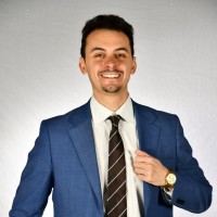
Principal Engineer
Current
Oct 2024 - Present
Please complete the CAPTCHA to continue

A concise factual answer block for searchers comparing this professional profile.
Nicolò Oliva is listed as Microelectronics engineer expert in project management, design, simulation and microfabrication. at II-VI Laser Enterprise Zürich, a with 46 employees, based in Biel, Berne, Switzerland. AeroLeads shows a matched LinkedIn profile for Nicolò Oliva.
Nicolò Oliva previously worked as Principal Engineer at Ii-Vi Laser Enterprise Zürich and Lead Engineer at Ii-Vi Laser Enterprise Zürich. Nicolò Oliva holds Doctor Of Philosophy - Phd, Electrical And Electronics Engineering from Epfl (École Polytechnique Fédérale De Lausanne).
This section adds company-level context without repeating Nicolò Oliva's masked contact details.
Review company-level records connected to Nicolò Oliva before choosing the right outreach path.
Highly motivated engineer with a electronics and physics background refined by four year experience in microfabrication, electronic devices design, simulation and characterization. I have worked and studied in four different countries, including the US, acquiring strong team building and international cooperation capabilities. I carried on multidisciplinary projects, cooperating directly with different universities and start ups. I am passionate about the development of commercial products with potential deep impact in our society and in the way we relate ourselves with technology. I speak fluently English and Italian, colloquial French and I am A2 in German.
Listed skills include Nanotechnology, Analog And Digital Design, Cadence, Originlab, and 15 others.
Company context helps verify the profile and gives searchers a useful next step.
A career timeline built from the work history available for this profile.


Lausanne Area, Switzerland
I focused my research activity on the development of 2D, 2D/3D and 2D/2D electronic devices. I designed reliable microfabrication processes for a variety of 2D materials, a deterministic transfer setup for polymer assisted assembly of heterojunctions and extensively characterized the electrical and optoelectrical performance of the fabricated devices. I acquired an extensive microfabrication expertise working in CMi, EPFL microfabrication facility, where I obtained habitation for a variety of deposition, etching, photlithography, ebeam lithography and characterization tools. During the extent of my project, I managed the available budget, I designed, negotiated and installed scientific setups and I established progressive research goals. Moreover, I trained and collaborated with two EPFL start-ups for the performance of wafer scale electrical and cryogenic measurements.

Pittsburgh, Stati Uniti
The target of my project was the analysis of the performance of two-port CMRs as piezoelectric MEMS transformers. In particular, these devices have been included in the design of an inductorless DC-DC power converter, to be demonstrated in a PCB implementation. The advantages of the investigated topology with respect to the traditional implementations of power converters are the elimination of the magnetic components, the considerable reduction in size and the CMOS compatibility of the resonators granted by a straightforward process flow. I developed an analytical model of two-port CMRs in order to estimate the achievable efficiency and voltage gains. Then I proposed a circuit topology for the DC-DC converter, that I validated with both an analytical model and simulations performed with ADS, a circuit simulator. From the results obtained, I identified the optimal characteristics of the resonators, and I proposed several CMR designs, with the aid of FEM simulations. The obtained devices, fabricated at the Carnegie Mellon nanofabrication facility, showed considerably high FOMs, granting good predicted efficiencies.

Grenoble Area, France
During my internship I focused on the study of electron-phonon coupling on few layers of 2H-TaS2, a two dimensional material with promising physical properties. In particular, I have realized the first thin samples exploiting the scotch taping technique Moreover, I have characterized their topography, evaluating the thickness on the base of a comparison between atomic force microscopy and Raman spectroscopy images. I also performed preliminary studies on the Raman spectrum of few layers samples under different illumination wavelengths, individuating the presence of both Kohn anomaly and resonant Raman scattering.
Other employees you can reach at laserenterprise.com. View company contacts for 46 employees →
 Max Steimle
Colleague at Ii-Vi Laser Enterprise ZürichGraubünden, Switzerland
View →
MS
Max Steimle
Colleague at Ii-Vi Laser Enterprise ZürichGraubünden, Switzerland
View →
MS
 Markus Schildenberger
Colleague at Ii-Vi Laser Enterprise ZürichZurich, Switzerland
View →
EC
Markus Schildenberger
Colleague at Ii-Vi Laser Enterprise ZürichZurich, Switzerland
View →
EC
 Elisabetta Corti
Colleague at Ii-Vi Laser Enterprise ZürichSwitzerland
View →
DF
Elisabetta Corti
Colleague at Ii-Vi Laser Enterprise ZürichSwitzerland
View →
DF
 Dirk Fokken
Colleague at Ii-Vi Laser Enterprise ZürichZurich, Switzerland
View →
AD
Dirk Fokken
Colleague at Ii-Vi Laser Enterprise ZürichZurich, Switzerland
View →
AD
 Alan(Xinli) Deng
Colleague at Ii-Vi Laser Enterprise ZürichZurich, Switzerland
View →
FA
Alan(Xinli) Deng
Colleague at Ii-Vi Laser Enterprise ZürichZurich, Switzerland
View →
FA
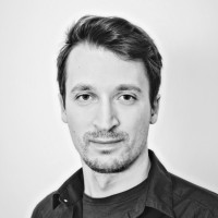 Faton Ameti
Colleague at Ii-Vi Laser Enterprise ZürichBuchs (Aargau), Aargau, Switzerland
View →
AR
Faton Ameti
Colleague at Ii-Vi Laser Enterprise ZürichBuchs (Aargau), Aargau, Switzerland
View →
AR
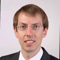 Aurelio Rossinelli
Colleague at Ii-Vi Laser Enterprise ZürichZurich, Switzerland
View →
MF
Aurelio Rossinelli
Colleague at Ii-Vi Laser Enterprise ZürichZurich, Switzerland
View →
MF
 Markus Feifel
Colleague at Ii-Vi Laser Enterprise ZürichZurich, Switzerland
View →
CC
Markus Feifel
Colleague at Ii-Vi Laser Enterprise ZürichZurich, Switzerland
View →
CC
 Carmine Colella
Colleague at Ii-Vi Laser Enterprise ZürichSwitzerland
View →
LC
Carmine Colella
Colleague at Ii-Vi Laser Enterprise ZürichSwitzerland
View →
LC
 Luca Castro Castell
Colleague at Ii-Vi Laser Enterprise ZürichZurich, Switzerland
View →
Luca Castro Castell
Colleague at Ii-Vi Laser Enterprise ZürichZurich, Switzerland
View →

Quick answers generated from the profile data available on this page.
Nicolò Oliva works for II-VI Laser Enterprise Zürich.
Nicolò Oliva is listed as Microelectronics engineer expert in project management, design, simulation and microfabrication. at II-VI Laser Enterprise Zürich.
Nicolò Oliva is based in Biel, Berne, Switzerland while working with II-VI Laser Enterprise Zürich.
Nicolò Oliva has worked for Ii-Vi Laser Enterprise Zürich, Abb, Hitachi Abb Power Grids, Epfl (École Polytechnique Fédérale De Lausanne), and Carnegie Mellon University.
Nicolò Oliva's colleagues at II-VI Laser Enterprise Zürich include Max Steimle, Markus Schildenberger, Elisabetta Corti, Dirk Fokken, and Alan(Xinli) Deng.
You can use AeroLeads to view verified contact signals for Nicolò Oliva at II-VI Laser Enterprise Zürich, including work email, phone, and LinkedIn data when available.
Nicolò Oliva holds Doctor Of Philosophy - Phd, Electrical And Electronics Engineering from Epfl (École Polytechnique Fédérale De Lausanne).
Nicolò Oliva is listed with skills including Nanotechnology, Analog And Digital Design, Cadence, Originlab, Microelectronics, Mems, Comsol, and Raman Spectroscopy.
Search by job title, company, industry, location, and seniority. Export verified B2B contact data when you need it.
Start free trial Search contactsCheck these profiles if this is not the Nicolò Oliva you were looking for.
View similar profiles