Incharge Instrumentation
Current
Sophisticated Analytical Instruments Laboratories Society
Apr 2024 - Present
Please complete the CAPTCHA to continue

A concise factual answer block for searchers comparing this professional profile.
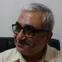
Pardeep Bhatia is listed as Nano Technologist || Material Characterization || Scanning Electron Microscopy || X-Ray Diffraction || NMR spectroscopy || Quality Control ISO 17025: 2017. at Thapar Institute of Engineering & Technology, based in Patiala, Punjab, India. AeroLeads shows a matched LinkedIn profile for Pardeep Bhatia.
Pardeep Bhatia previously worked as Incharge Instrumentation at Sophisticated Analytical Instruments Laboratories Society and Senior scientific assistant at Thapar Institute Of Engineering & Technology. Pardeep Bhatia holds Master'S Degree, Nanotechnology, First from Punjabi University.
This section adds company-level context without repeating Pardeep Bhatia's masked contact details.
Review company-level records connected to Pardeep Bhatia before choosing the right outreach path.
To build a career in the field of Nano technological research, consistent academic record with zeal to learn new concepts and innovative ideas for achieving best results. Motivated, self-starter with a passion to succeed and desire to excel in the area of advanced sciences that would enable me to develop professional, analytical, logical skills, & a challenging career ahead.
Company context helps verify the profile and gives searchers a useful next step.

A career timeline built from the work history available for this profile.
Patiala, Punjab, India

Patiala, Punjab, India

Ropar, Punjab, India

Activities and Societies: National Cadet Corpse
Quick answers generated from the profile data available on this page.
Pardeep Bhatia works for Thapar Institute of Engineering & Technology.
Pardeep Bhatia is listed as Nano Technologist || Material Characterization || Scanning Electron Microscopy || X-Ray Diffraction || NMR spectroscopy || Quality Control ISO 17025: 2017. at Thapar Institute of Engineering & Technology.
Pardeep Bhatia is based in Patiala, Punjab, India while working with Thapar Institute of Engineering & Technology.
Pardeep Bhatia has worked for Sophisticated Analytical Instruments Laboratories Society, Thapar Institute Of Engineering & Technology, Thapar University, Auriga Laboratories, and Guru Gobind Singh Super Thermal Plant.
You can use AeroLeads to view verified contact signals for Pardeep Bhatia at Thapar Institute of Engineering & Technology, including work email, phone, and LinkedIn data when available.
Pardeep Bhatia holds Master'S Degree, Nanotechnology, First from Punjabi University.
Search by job title, company, industry, location, and seniority. Export verified B2B contact data when you need it.
Start free trial Search contactsCheck these profiles if this is not the Pardeep Bhatia you were looking for.