Process Development
Semiconductor Industry
Please complete the CAPTCHA to continue
@yahoo.in
✓
LinkedIn matched
A concise factual answer block for searchers comparing this professional profile.
Pawan Kumar is listed as Process Development at Semiconductor Industry, based in Vancouver, British Columbia, Canada. AeroLeads shows a work email signal at yahoo.in and a matched LinkedIn profile for Pawan Kumar.
Pawan Kumar previously worked as Process Engineer at Semiconductor Industry and Scientist at Semiconductor Industry. Pawan Kumar holds Indo French Visiting Fellowship (Raman Charpak) For 6 Month, Chemistry from University Of Lille 1 Sciences And Technology.
This section adds company-level context without repeating Pawan Kumar's masked contact details.
AeroLeads found 1 current-domain work email signal for Pawan Kumar. Compare company email patterns before reaching out.
Developing protocol, and process control for semiconductor device optimization. Thin film development, inorganic etchable protection layer, development of etchant, measurement of device.Previous experience:• Experience in the fabrication and development of new semiconductors, 2D materials, and hybrid catalysts using wet/solid-state synthesis for electrocatalysis, photocatalysis, organic synthesis, optoelectronics and photovoltaics. • Two-year industrial experience in leading semiconductor, and FMCG companies. Responsible for process optimization, data analysis, data collection, Raw and finished product quality check, report preparation, and managing teams. • Five years of hand-on experience in various advanced materials synthesis and material characterization techniques. Modulation of electronic bandgap, defect engineering, surface functionalization, molecular/atomic level control on catalysts design, reactor design, electrochemical/electrical data collection using various applications and chemical knowledge to make critical decisions• Passionate about learning and solving complex problems using analytical skills. Collaborated with >50 scientists and diverse networks. Expertise and skills- Materials synthesis, 2D materials synthesis and modification, single atom catalysts (SACs), 2D-2D Vander Waal heterostructures: graphene, graphene oxides, TiO2/ZnO nanotubes/nanorods, carbon nitride, black phosphorous, MXene, WS2, MoS2.- electrocatalysis, photo/electrocatalysis, CO2 reduction, CH4 oxidation, microplastic oxidation, biomass conversion. - Instruments/data interpretation expert: XPS, EELS, NMR, ssNMR, XRD, XAS (XANES, EXAFS, SAXS, WAXS), TRPL, KPFM, electrochemical studies (EIS, Mott-Schottky, surface coverage, photocurrent measurement, electrode fabrication), HPLC, GC, GC-MS, UV-Vis, DLS, FE-SEM, TEM, Potentiostat, FTIR, Raman, Fluorescence spectroscopy, Karl-Fischer, optical rot
Listed skills include Chemistry, Spectroscopy, Hplc, Analytical Chemistry, and 21 others.
Company context helps verify the profile and gives searchers a useful next step.

A career timeline built from the work history available for this profile.
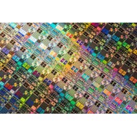
Vancouver, British Columbia, Canada
Process development to improve the performance of semiconductor devices
Calgary, Alberta, Canada
• Worked on a $75 million Government of Canada project to develop materials for transition to a net-zero carbon economy.• Developed new carbon-based semiconductor materials and single atom catalysts and their thin films with tuned photophysical properties and coordination pattern for photo/electrocatalysis, photocatalysis, and selective conversion.• Record >300h stability and 10 wt% single atoms concentration for Co-based graphenic electrode in electrocatalysis.• Recognizing the importance of single atom-based semiconductors for various applications Canadian synchrotron facility awarded user access for the XAS characterization (most advanced technique for materials characterization)

Edmonton, Canada Area
• Developed numerous semiconductors structures such as TiO2/WS2/BiOI/perovskites/SnIP/CuIP/Black P/carbon nitride, nanotubes, nanorods, nanoflowers, thin-film for optoelectronics and photo/electrochemical applications.• Access at Nanofab (Canada's second-largest nanofabrications facility) and the National Institute of Nanotechnology, NINT (North America's largest nanotechnology center) for the advanced characterization of materials.Received collective 20000 CAD funding from CMC microsystems for the fabrications and characterization of materials.• Fabricated solar cells, memory, and electrochemical devices using E-beam evaporation sputtering, PLD, and ALD, evaluated electrical/electronic properties and characterized devices with various techniques.• Collaborated with various groups on diverse research topics and successfully delivered 10+ projects• Developed the first low band gap azo-linked C3N5 organic semiconductor for the electron transport layer in photovoltaics.• Received Emerging Material Chemistry Investigator Award by the Canadian Society for Chemistry/IUPAC (North America level) for significant contribution to the field of Materials Chemistry.• Mentored/supervised 12+ Master's/Ph.D. students from Germany, India, Canada, Columbia, and China. 2 Ph.D. thesis and 4 Master’s thesis directly acknowledges my contribution as co-supervisor.

District Olomouc, Czech Republic
• Spearheaded projects to design magnetic/graphenic materials with high selectivity resulting in 4 successful projects.• Developed the first cyanographene graphene with 15% nitride functionalization and pinned 1% Cu atoms in a mixed valence state reaching 99% product selectivity.• Submitted funding proposal for the Czech Academy of Science in collaboration with US-EPA scientists.
Dehra Dun Area, India
• Produced and completed the project on "Development of novel catalytic systems for the photoreduction of CO2 to fuel and chemicals"• Worked on various metal complexes and semiconductor materials for organic catalysis, and photocatalysis.• Led>10 projects and successfully delivered >20 research articles• Worked in collaboration with the national and international acclaimed scientists.• Mentored >6 undergraduate and master's students and help them to disseminate research articles. They are part of reputed organizations such as IBM, and McGill, Binghamton University• Part of the team for 3 international grant proposals (Indo-French, Indo-Polish, DST-JSPS)
Pune Area, India
• Worked on nanomaterials development for toxic chemicals detection and degradation technologies• Collaborated with Tata Research Development and Development center (TRDDC) Scientists and developed an inflatable shelter that can be used on-site.• Led projects, write reports, and provide suggestions to a team of engineers, presented results to wide audience in a simplified way
Haridwar Area, India
• Chemical analysis and quality check of raw materials and finished goods maintaining reports in the ERP system.• Follow standard SOPs, ensure good laboratory practices, and coordinated with the production department and suppliers.
Naini Tal Area, India
• Analyzed, reviewed and delivered data on various samples of raw and finished goods

Worked at the Institute of Electronics, Microelectronics and Nanotechnology.
Activities and Societies: Catalysts for organic transformation, photocatalysis, CO2 reduction, and H2 generation.• Worked on various metal.
• Learned organizational structure and management, human resource management • Deeply focused course on case studies for various leading.
• A special master course designed for industry, combining the analytical chemistry and industrial chemistry • Learned techniques used.
Quick answers generated from the profile data available on this page.
Pawan Kumar works for Semiconductor Industry.
Pawan Kumar is listed as Process Development at Semiconductor Industry.
AeroLeads has found 1 work email signal at @yahoo.in for Pawan Kumar at Semiconductor Industry.
Pawan Kumar is based in Vancouver, British Columbia, Canada while working with Semiconductor Industry.
Pawan Kumar has worked for Semiconductor Industry, University Of Calgary, University Of Alberta, Palacký University Olomouc, and Indian Institute Of Petroleum.
You can use AeroLeads to view verified contact signals for Pawan Kumar at Semiconductor Industry, including work email, phone, and LinkedIn data when available.
Pawan Kumar holds Indo French Visiting Fellowship (Raman Charpak) For 6 Month, Chemistry from University Of Lille 1 Sciences And Technology.
Pawan Kumar is listed with skills including Chemistry, Spectroscopy, Hplc, Analytical Chemistry, Uv/Vis, Characterization, Materials Science, and Research.
Search by job title, company, industry, location, and seniority. Export verified B2B contact data when you need it.
Start free trial Search contactsCheck these profiles if this is not the Pawan Kumar you were looking for.