Frank Lee

Frank Lee Email and Phone Number

Senior PCB Technical Support | EMS ODM OEM Consultant | FAE SQE Consultant @ Kington Precision Electronics Co., Ltd
shenzhen, guangdong, china
Frank Lee's Location
Shenzhen, Guangdong, China, China
About Frank Lee

Frank Lee is a Senior PCB Technical Support | EMS ODM OEM Consultant | FAE SQE Consultant at Kington Precision Electronics Co., Ltd. He possess expertise in pcb design, pcb layout, pcb fabrication, pcb assembly, allegro design and 14 more skills.

Frank Lee's Current Company Details
Kington Precision Electronics Co., Ltd

Kington Precision Electronics Co., Ltd

View
Senior PCB Technical Support | EMS ODM OEM Consultant | FAE SQE Consultant
shenzhen, guangdong, china
Website:
kingtontech.com
Employees:
6
Frank Lee Work Experience Details
  • Kington Precision Electronics Co., Ltd
    Sqe | Fae | Pcb Design Layout | Pcb Fab And Quality Specialist
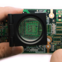
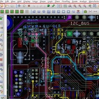
    Kington Precision Electronics Co., Ltd Jan 2020 - Present
    Shenzhen, Guangdong, China
    Skill and experience:1) Be familiar IPC-6102, IPC-4101,IPC-600 standard and understanding customer technical requirement,design purpose, Gerber file, specification etc and solve any capability and manufacturability problems of PCB.2) With 16 years of PCB engineering and quality experience, can use wide rang PCB software such as Altium,Protel99SE,Pads,Eagle,Genesis 2000,CAM350.Can make PCB design rule check and DFM analysis.3) Master the PCB fabrication of metal PCB, Heavy Copper… Show more Skill and experience:1) Be familiar IPC-6102, IPC-4101,IPC-600 standard and understanding customer technical requirement,design purpose, Gerber file, specification etc and solve any capability and manufacturability problems of PCB.2) With 16 years of PCB engineering and quality experience, can use wide rang PCB software such as Altium,Protel99SE,Pads,Eagle,Genesis 2000,CAM350.Can make PCB design rule check and DFM analysis.3) Master the PCB fabrication of metal PCB, Heavy Copper PCB, ImpedanceControl, High Frequency (RF) high speed, HDI blind and buried via board , Multi-layer PCB. Rigid-flex PCB, Flexible PCB. Know about the CCL raw material specification, such as FR-4, CEM-3, Rogers, Isola and etc.4)Experienced in drill process, pressure process, image transfer, DES line process, etching process, plating , solder mask printed(D/F), surface treatment ,CNC process, test process and etc.5) Rich experience in impedance controlled, stackup.Use Polar software to calculate the value and advise a best solution to customers.6) Familiar the factory audit process.7) Familiar the PCB acception standard.8) PCB assembly, including solder paste application, component placement, reflow soldering, and testing.9) Value-added Technical Support> DFM(design for manufacturability ) analysis> DRC analysis> Optimized stackup design> Impedance matching calculate > Small pitch BGA design case (less than 0.5mm pitch)> VIA ON PAD technology > HDI technology > Sepcial PCB, special material support> FPC stackup and material design support> Flex-Rigid PCB design rule > Metal core PCB design rule > High frequency PCB design> DFEMA (Design Failure Mode and Effect Analysis) analysis on GerberBOM and Components option:> Components parameter checking with datasheet> Out of stock components search> Footprint checking with datasheet> Pick&Place file check with Gerber> Hard and old parts checking and sourcing> Alertnative parts verify Show less
  • Kington Precision Electronics Co., Ltd
    Senior Pcb Technical Sale | Pcb Manufacture | Pcb Assembly
    Kington Precision Electronics Co., Ltd Feb 2016 - Dec 2019
    Shenzhen, Guangdong, China
    Develop the customers who need PCB/PCBA;Service customers with my technical and profesional skill to solve the questions before release PCB/PCBA order ;Check customer Gerber file and BOM;Quote to customers;Follow the order fabrication and delivery schedule;Communicate with customers for the DFM ayalysis and FEMA;Cost evaluation with customer for their design;Help customer to choose the suitable component that is easy to source and cost-effective;
  • Kington Precision Electronics Co., Ltd
    Senior Pcb Designer
    Kington Precision Electronics Co., Ltd May 2013 - Jan 2016
    Shenzhen, Guangdong, China
    In KINGTON, I am a senior PCB design engineer to provide Printed Circuit Board layout design services of Rigid PCB, Flex PCB, Rigid-Flex PCB to companies that develop and/or manufacture electronic products for automotive, military, aerospace/avionics, telecommunications, computer hardware, consumer electronics, and medical device applications. We are dedicated to providing quality PCB Layout Design services utilizing experienced designers, at affordable rates, in a timely manner… Show more In KINGTON, I am a senior PCB design engineer to provide Printed Circuit Board layout design services of Rigid PCB, Flex PCB, Rigid-Flex PCB to companies that develop and/or manufacture electronic products for automotive, military, aerospace/avionics, telecommunications, computer hardware, consumer electronics, and medical device applications. We are dedicated to providing quality PCB Layout Design services utilizing experienced designers, at affordable rates, in a timely manner. Job Summary: Responsible for PCB (Printed Circuit Board) layout design of CPU (Central Processing Unit) modules / IO (Input/Output) modules / communication boards / image processing modules / chassis to system integration, prototyping and mass production, and bring the output to the market. Design placement for main chipsets in main board. Expert with PCB layout with PCI-Express, USB, SATA, high speed memory (DDR, DDR2, DDR3, DDR4) and high density interconnect. Primary Job Responsibilities: ● Analysis the input from customer and providing pre quote to the design. ● On Quote approval, Responsible for handling the tasks like analyzing the inputs from customers, creating schematic, Preparing the Bill of Materials ● Analyze the design in Probecard, Dutboards, Direct docking, completely from the SPEC given from the customer based on tester specifications ● Analyzed process through logical reasoning & provided technical support, if necessary. ● Perform responsibilities of designing layout process and creating component footprints. ● Performed the task of coordinating the team in designing layout process. ● Responsibilities for ensuring that hardware layouts are designed as per design standards. ● Gerber Generation and validation of BASIC DFM specification on it. ● Ensuring On-time Project schedule and delivery. Show less
  • Scc Circuit Co.,Ltd
    Senior Pcb Designer
    Scc Circuit Co.,Ltd Oct 2009 - Jan 2013
    Shenzhen, Guangdong, China
    Design Skills & Projects: • PCB CAD: ORCAD ALLEGRO, ALTIUM, PADS, CAM : CAM350, GENESIS2000• Controlled Impedance layout: strip-line, micro-strip, single, dual, symmetrical and offset, differential signal pair, matched-length manual and auto-routing techniques, necessary for successful implementation of critical Datacom test equipment circuitry. • Analog, digital and mixed-signal design layout, double sided high-density SMT. • Multi-layer PCB layout (up to 30 layers or more) for… Show more Design Skills & Projects: • PCB CAD: ORCAD ALLEGRO, ALTIUM, PADS, CAM : CAM350, GENESIS2000• Controlled Impedance layout: strip-line, micro-strip, single, dual, symmetrical and offset, differential signal pair, matched-length manual and auto-routing techniques, necessary for successful implementation of critical Datacom test equipment circuitry. • Analog, digital and mixed-signal design layout, double sided high-density SMT. • Multi-layer PCB layout (up to 30 layers or more) for complex designs with flex-rigid PCB design.• Distributed/Buried Capacitance PCB stack-up (ZBC-2000) allowed design layout to reduce decoupling capacitor count and thereby also saving assembly time. • BGA (Ball Grid Array), QFP (Quad Flat Pack) devices implemented to allow for high-density designs and efficient packaging of circuitry on smaller boards. • EMI considerations in layout of critical PCBs; “Copper pour” ground plane on external layers and ground stitching for shielding, resulting in product’s EMI compliance. • DFM (Design for Manufacturability) for easier, cost-effective assembly and DFT (Design for Testability) process for reliable, error-free bed-of-nails testing of the circuitry. • Library parts creation and maintenance Accomplishments: • Successfully managed all aspects of PCB layout design process and implementation by meeting scheduling milestones with cost-effective solutions. • Layout process development, including data transfer from schematic through to completion of layout, procurement of prototype PCBs and managing outsourcing of layout when required for the most efficient use of resources. • Demonstrated a high level of adaptability and organizational skill in managing a wide variety of PCB layout designs. Devised and implemented a Design checklist to improve process flow in order to help spot critical design issues early and thus reduce or eliminate possible costly redesigns. Show less
  • Fastprint Circuit
    Pcb And Pcb Assembly Service Engineer
    Fastprint Circuit Jan 2007 - Apr 2009
    Shenzhen, Guangdong, China
    Job Summary: • Analyse circuit diagrams and electrical code to determine wiring layouts for the functionality • Request netlist, data source name, rule file, drawing interchange file, mechanical engineers file, guideline, and stack up from the electrical engineer and mechanical engineers • Ensure components are working. Import all the given files on the board. Update netlist, rule file, and DXF (Drawing Interchange File) file respectively. Set the stack-up based on the given file… Show more Job Summary: • Analyse circuit diagrams and electrical code to determine wiring layouts for the functionality • Request netlist, data source name, rule file, drawing interchange file, mechanical engineers file, guideline, and stack up from the electrical engineer and mechanical engineers • Ensure components are working. Import all the given files on the board. Update netlist, rule file, and DXF (Drawing Interchange File) file respectively. Set the stack-up based on the given file after the procedure has been established. • Administer layout process (1) placement (2) routing high-speed signals, non-critical traces and power (4) length matching (5) trace clean-up (6) DRC (7) power check process. • Works closely with (1) Hardware Engineers in the creation of schematic circuits, (2) Power and manufacturing Engineers (3) Senior Engineer for final checking • Generate the final files which include CAD (Computer Aided Design), SMD (Surface Mount Device), board, SPC (Statistical Process Control) and notice. After sorting all the folders, prepare the folder for notice and SMD. • Ask all function team to sign off the PDM (Product Data Management) form. Check and monitor the process using programs such as CAM350 (Computer-Aided Manufacturing) and Valor. SKILLS ➢ Ability to do schematic capture ➢ Knowledge in creating components to be used in design ➢ Expert in routing high speed nets (USB, PCIE, DDR, SDRAM, SATA, LAN) ➢ In-depth knowledge in PCB design analysis, signal integrity and transmission line circuitry ➢ Outstanding knowledge of analog testing and debugging techniques ➢ Ability to supply full set of deliverables for PCB fab and assembly ➢ Wide experience in Allegro Cadence tool, CAM 350, Valor Fabrication, Vsure fabrication, Atium Designer ➢ Ability to co-work well in other costumer and the functional teams such as EE, EMI, RF, ANALOG➢ Outstanding knowledge of RF, analog, digital antenna and audio signals ➢ Expert in Handling HDI project Show less

Frank Lee Skills

Pcb Design Pcb Layout Pcb Fabrication Pcb Assembly Allegro Design Altium Designer Eagle Designer Hardware Development Ipc6012 Firware Development Schematic Capture Emc Compliance Npi Management Schematic Design Emc Analysis Smt Reverse Engineering Altium Design Pcb Eagle Pcb Design

Frequently Asked Questions about Frank Lee

What company does Frank Lee work for?

Frank Lee works for Kington Precision Electronics Co., Ltd

What is Frank Lee's role at the current company?

Frank Lee's current role is Senior PCB Technical Support | EMS ODM OEM Consultant | FAE SQE Consultant.

What skills is Frank Lee known for?

Frank Lee has skills like Pcb Design, Pcb Layout, Pcb Fabrication, Pcb Assembly, Allegro Design, Altium Designer, Eagle Designer, Hardware Development, Ipc6012, Firware Development, Schematic Capture, Emc Compliance.

Who are Frank Lee's colleagues?

Frank Lee's colleagues are Lee L., Leo Yan, Debby Ly, Dieu Thuy, Dillon Yan.

Not the Frank Lee you were looking for?

  • Frank Lee

    Principle Product Manager At Microsoft
    Beijing, China
    1
    hotmail.com
  • Frank Lee

    Nio蔚来 - Hr
    Haidian District
  • 1
    163.com
  • Frank Lee

    Xuhui District
  • Frank Lee

    I Was Working As Different Kind Of Roles In The Industry, For Example Customer Service Specialist, Bd, Operation Manager, Coo. Currently Looking For A Remote Job In Crypto Industry.
    Jing'an District

Free Chrome Extension

Find emails, phones & company data instantly

Find verified emails from LinkedIn profiles
Get direct phone numbers & mobile contacts
Access company data & employee information
Works directly on LinkedIn - no copy/paste needed
Get Chrome Extension - Free

Aero Online

Your AI prospecting assistant

Download 750 million emails and 100 million phone numbers

Access emails and phone numbers of over 750 million business users. Instantly download verified profiles using 20+ filters, including location, job title, company, function, and industry.