
AeroLeads people directory · profile
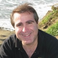
Peter Cirigliano Email & Phone Number
Product and Process Development Engineer
at
Endevco
1 work email found
@endevco.com
LinkedIn matched
✓ Verified August 2026
4 data sources
Profile completeness 100%
Current company
Role
Product and Process Development Engineer
Location
Sunnyvale, California, United States
Company size
Who is Peter Cirigliano? Overview
A concise factual answer block for searchers comparing this professional profile.
Quick answer
Peter Cirigliano is listed as Product and Process Development Engineer at Endevco, a with 815 employees, based in Sunnyvale, California, United States. AeroLeads shows a work email signal at endevco.com and a matched LinkedIn profile for Peter Cirigliano.
Peter Cirigliano previously worked as Product/Process Development Engineer at Endevco and Dry Etch Engineer (Temporary, Project-Based) at Tsi Semiconductors. Peter Cirigliano holds Bs, Engineering Chemistry from Stony Brook University.
Company email context
Email format at Endevco
This section adds company-level context without repeating Peter Cirigliano's masked contact details.
{last}@endevco.com
86% confidence
AeroLeads found 1 current-domain work email signal for Peter Cirigliano. Compare company email patterns before reaching out.
Profile bio
About Peter Cirigliano
A process engineer with the semiconductor industry with experience in etch, photolithography and pattern shrink. Developed processes for standard CMOS logic/memory, MEMS, TSV, photonics, sensors, MTJ, biotech and novel memory. Also, has experience in failure analysis (FA) and characterization support for lithium-ion battery (silicon anode-based) development.Specialties: Process development or improvement, customer/application support, dry (plasma) or wet etch, photolithography, lithium-ion battery failure analysis.
Listed skills include Design Of Experiments, Semiconductors, Metrology, Etching, and 28 others.
Current workplace
Peter Cirigliano's current company
Company context helps verify the profile and gives searchers a useful next step.
Endevco
12 roles · 44 years
Peter Cirigliano work experience
A career timeline built from the work history available for this profile.
Product/Process Development Engineer
CurrentEndevco (formerly Meggitt Sensing Systems) specializes in designing products to operate under harsh and demanding conditions. Our systems are used in a diverse range of markets and applications, from aircraft and space launchers to gas turbines and heart monitors. Improved or developed various manufacturing processes in our MEMS sensors wafer fab. Played a key role in transferring frontend assembly for PR/pressure devices and testing of VC devices from our home facility during divestiture of our division to new ownership. Generated new run cards, procedural documents as well as operation spec and training for new die assembly tool for this purpose.
Jun 2018 - Present

Dry Etch Engineer (Temporary, Project-Based)
Temporary, project-based employment, for up to 6 months, working on various dry plasma etch development or improvement projects for a company that does CMOS foundry manufacture as well as custom integration development for various customers.
Oct 2016 - Jun 2018

Sr Principal Engineer
Developed or improved or implemented failure analysis (FA) techniques in the post-mortem evaluation of new generation silicon anode-based lithium-ion cells using Xray, thermal imaging, electrical probing, encapsulation/saw/polish/SEM, evaluations of cyclic voltammograms and full tear downs of completed cells or in-process test structures or vehicles.
Aug 2013 - Sep 2016
Principal Process Engineer
Tasked with the startup, qualification and ownership of several transferred etch tools from acquisition for use in a customer integration/process development program. Supported main foundry CMOS dry etch issues and development as well as external “more than Moore” customer needs and projects.
Feb 2013 - Aug 2013

Etch Engineer
Developing new etch applications for a wide variety of client customers, such as novel memory and logic, biotech, MEMS, photonics, sensors, solar, TSV, and other nascent technologies, using DOE methodology to produce robust and manufacturable processes. Projects involve a variety of etch and metrology tools, substrate types, and novel integration schemes.
Jul 2010 - Sep 2012
Volunteer And Member
Promatch
Oct 2009 - May 2010
Staff Process Engr - Patterning Group
Pivotal role in the development of processes and support of key customer for a new plasma-based pattern shrink chamber which led to first revenue penetration of product. Collaborated with European consortium to develop shrink techniques to enable 65nm and smaller technology nodes which led to joint authoring of three publications in the industry trade organizations. Met with and presented updates to customer on a regular basis as well as performed on-site development support.
2006 - 2009
~3 yrs
Staff Process Engr- Dielectric Etch
Collaborated with alliance partner to develop OSG low-k dielectric etch processes. Developed and used novel techniques to study dielectric damage of OSG and organic low-k films during resist strip. Lead engineer in JDP effort with a resist manufacturer in developing bilayer dry develop and etch processes which resulted in being an invited guest speaker at the manufacturer’s corporate symposium in Europe and the primary co-author of a published article. Working with hardware, design and equipment support in a small group, provided the process development for the Lam 4520XL chamber which became an industry workhorse. Generated the process release document that became a reference document in the field. Managed a small project group for development of high-aspect ratio contact processes on the Lam Exelan HP. Made extensive use of Design of Experiment (DOE) techniques to develop or fine tune processes.
1995 - 2006
~11 yrs

Sr. Process Engineer
Developed and supported photolithographic processes using projection alignment, spin tracks, and various wet and dry etch systems. Wrote and maintained process specifications that were used to train line operators and equipment support staff and were used as reference documents on the manufacturing line. Employed SPC techniques to control fab line process, monitoring Cp and Cpk.
1983 - 1995
~12 yrs
Litho & Etch Process Engineer
Lsi Logic
1983 - 1994
~11 yrs
Process Engineer
Lsi Logic
1983 - 1994
~11 yrs
Team & coworkers
Colleagues at Endevco
Other employees you can reach at pcb.com. View company contacts for 815 employees →
DP
 Dan Peng
Colleague at EndevcoBuffalo-Niagara Falls Area, United States
View →
WB
Dan Peng
Colleague at EndevcoBuffalo-Niagara Falls Area, United States
View →
WB
 Wolfgang Buechler
Colleague at EndevcoNiagara County, New York, United States
View →
JS
Wolfgang Buechler
Colleague at EndevcoNiagara County, New York, United States
View →
JS
 Jessica Shvimer
Colleague at EndevcoGrand Island, New York, United States
View →
LB
Jessica Shvimer
Colleague at EndevcoGrand Island, New York, United States
View →
LB
 Larry Busch
Colleague at EndevcoStrykersville, New York, United States
View →
RS
Larry Busch
Colleague at EndevcoStrykersville, New York, United States
View →
RS
 Ralph Shoberg
Colleague at EndevcoFarmington, Michigan, United States
View →
DC
Ralph Shoberg
Colleague at EndevcoFarmington, Michigan, United States
View →
DC
 Dan Cilibia
Colleague at EndevcoDepew, New York, United States
View →
杨
Dan Cilibia
Colleague at EndevcoDepew, New York, United States
View →
杨
 杨宗霖
Colleague at EndevcoDongcheng District, Beijing, China
View →
AK
杨宗霖
Colleague at EndevcoDongcheng District, Beijing, China
View →
AK
 Amanda Keicher
Colleague at EndevcoBuffalo-Niagara Falls Area, United States
View →
AH
Amanda Keicher
Colleague at EndevcoBuffalo-Niagara Falls Area, United States
View →
AH
 Assad Harris
Colleague at EndevcoBuffalo, New York, United States
View →
RB
Assad Harris
Colleague at EndevcoBuffalo, New York, United States
View →
RB
 Robin Burgess
Colleague at EndevcoHalifax, North Carolina, United States
View →
Robin Burgess
Colleague at EndevcoHalifax, North Carolina, United States
View →
Dan Peng
Colleague at EndevcoBuffalo-Niagara Falls Area, United States
View →
WB
Wolfgang Buechler
Colleague at EndevcoNiagara County, New York, United States
View →
JS
Jessica Shvimer
Colleague at EndevcoGrand Island, New York, United States
View →
LB
Larry Busch
Colleague at EndevcoStrykersville, New York, United States
View →
RS
Ralph Shoberg
Colleague at EndevcoFarmington, Michigan, United States
View →
DC
Dan Cilibia
Colleague at EndevcoDepew, New York, United States
View →
杨
杨宗霖
Colleague at EndevcoDongcheng District, Beijing, China
View →
AK
Amanda Keicher
Colleague at EndevcoBuffalo-Niagara Falls Area, United States
View →
AH
Assad Harris
Colleague at EndevcoBuffalo, New York, United States
View →
RB
Robin Burgess
Colleague at EndevcoHalifax, North Carolina, United States
View →
2 education records
Peter Cirigliano education

Bs, Engineering Chemistry
Education record
Various Training: Software, Oem, Professional Development, Analytical, Doe, Spectranalysis, Etc.
FAQ
Frequently asked questions about Peter Cirigliano
Quick answers generated from the profile data available on this page.
What company does Peter Cirigliano work for?
Peter Cirigliano works for Endevco.
What is Peter Cirigliano's role at Endevco?
Peter Cirigliano is listed as Product and Process Development Engineer at Endevco.
What is Peter Cirigliano's email address?
AeroLeads has found 1 work email signal at @endevco.com for Peter Cirigliano at Endevco.
Where is Peter Cirigliano based?
Peter Cirigliano is based in Sunnyvale, California, United States while working with Endevco.
What companies has Peter Cirigliano worked for?
Peter Cirigliano has worked for Endevco, Tsi Semiconductors, Enovix Corp., Svtc, and Promatch.
Who are Peter Cirigliano's colleagues at Endevco?
Peter Cirigliano's colleagues at Endevco include Dan Peng, Wolfgang Buechler, Jessica Shvimer, Larry Busch, and Ralph Shoberg.
How can I contact Peter Cirigliano?
You can use AeroLeads to view verified contact signals for Peter Cirigliano at Endevco, including work email, phone, and LinkedIn data when available.
What schools did Peter Cirigliano attend?
Peter Cirigliano holds Bs, Engineering Chemistry from Stony Brook University.
What skills is Peter Cirigliano known for?
Peter Cirigliano is listed with skills including Design Of Experiments, Semiconductors, Metrology, Etching, Spc, Semiconductor Industry, Plasma Etch, and Process Simulation.
Find 750M verified contacts
Search by job title, company, industry, location, and seniority. Export verified B2B contact data when you need it.
Start free trialPeople with similar names
Check these profiles if this is not the Peter Cirigliano you were looking for.
View similar profiles


