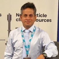

Rommel Paulo Viloan
AeroLeads people directory · profile

Rommel Paulo Viloan Email & Phone Number

Development Engineer | Materials Scientist and Engineer | PVD process and coatings engineer at Ionautics
Location: Linköping, Östergötland County, Sweden 7 work roles 3 schools
LinkedIn matched
✓ Verified August 2026 3 data sources Profile completeness 100%

Contact Signals

LinkedIn Profile matched
3 free lookups remaining · No credit card
Current company
Role
Development Engineer | Materials Scientist and Engineer | PVD process and coatings engineer
Location
Linköping, Östergötland County, Sweden
Company size

Who is Rommel Paulo Viloan? Overview

A concise factual answer block for searchers comparing this professional profile.

Quick answer

Rommel Paulo Viloan is listed as Development Engineer | Materials Scientist and Engineer | PVD process and coatings engineer at Ionautics, a with 7 employees, based in Linköping, Östergötland County, Sweden. AeroLeads shows a matched LinkedIn profile for Rommel Paulo Viloan.

Rommel Paulo Viloan previously worked as Development Engineer at Ionautics and Postdoctoral Researcher at Link��Ping University. Rommel Paulo Viloan holds Phd, Materials Science from Linköping University.

Company email context

Email format at Ionautics

This section adds company-level context without repeating Rommel Paulo Viloan's masked contact details.

Ionautics

Review company-level records connected to Rommel Paulo Viloan before choosing the right outreach path.

Profile bio

About Rommel Paulo Viloan

I am a materials engineer and scientist with ~15 years of experience in various thin film deposition technologies (PVD - triode sputtering, magnetron sputtering, HiPIMS, hollow cathode and arc evaporation) in industrial and research laboratory settings. Throughout the years, I obtained significant experiences in surface treatment, coating solutions, materials development and characterization, product, and equipment development. I have a proven record in managing research projects, process engineering and materials analysis. I am inclined towards increasing efficiency at work through automation of data analysis and utilizing six sigma principles.

Listed skills include Thin Films, Characterization, Semiconductors, Sputtering, and 16 others.

Current workplace

Rommel Paulo Viloan's current company

Company context helps verify the profile and gives searchers a useful next step.

Ionautics
Ionautics
Development Engineer | Materials Scientist and Engineer | PVD process and coatings engineer
ase, vasternorrlands lan, sweden
Website
Employees
7
AeroLeads page
7 roles

Rommel Paulo Viloan work experience

A career timeline built from the work history available for this profile.

Development Engineer

Current

Linköping, Ostergotland County, Sweden

Contributing to a more sustainable future by developing catalyst nanoparticles for hydrogen generation. Material growth is achieved through pulsed plasmas, with the resulting particles primarily analyzed using x-ray diffraction and electron microscopy techniques.Responsibilities:• Process scaling-up• Process engineering to improve material collection• Process development for catalyst material development• Method development for nanoparticle quantification• Material and process characterization

Jan 2022 - Present

Phd Researcher

Linkoping, Sweden

Responsible for investigating a new coating process based on HiPIMS. Maintenance and improvement of vacuum chambers and associated parts. Management of research projects. Introduction and training of new staff, visiting scientist and students to various equipment and material analysis techniques.Key accomplishments:• Publication of peer-reviewed articles in reputable scientific journals (4 as first author and 3 as co-author).• Presentation of research in various international conferences and meetings (4).• Experimental verification of new thin film deposition technique using ion mass spectrometry and thin film deposition.• Automation of mass spectrometer data analysis using Python to reduce data processing time from hours to seconds.

Sep 2016 - Jun 2021

Engineer

Beta Nanocoating Philippines, Inc.

Calamba, Laguna, Philippines

Overall technical support for PVD coating process and surface preparation processes, which includes knowledge generation, process engineering, staff training and contacting suppliers. Interfacing with clients and point person for client-issue resolution. Planning of production department activities. Drive management meetings for updating the status of projects with clients, equipment condition and brainstorming.Key accomplishments:• Proposed alternative suppliers with the goal of bringing down cost while maintaining product quality.• Initiated communication with potential clients, which resulted in several coating trials and repeat orders.• Provided technical expertise and personnel training for a client under a technology transfer framework.• Managed production raw materials by determining ordering points based on raw material consumption calculations.• Resolved issues with QA equipment by identifying defective parts of microscope, placing orders for replacement and boost capability by introducing new equipment.

Oct 2014 - Aug 2016

Material Analyst

Department Of Science And Technology - Admatel

• Electron microscopy (SEM), elemental analysis (EDS) and FIB milling to support client’s failure analysis activities and research.• Communicated with equipment supplier for preventive maintenance and issue resolution.

Apr 2014 - Oct 2014

Science Research Specialist

National Institute Of Physics, Philippines

Quezon City, National Capital Region, Philippines

Lead a laboratory subgroup composed of 1 PhD student, 2 MS students and 1 BS student with primary responsibilities in training, ensuring that research is in line with laboratory projects and extending assistance in research works.3D modeling of parts and assemblies using Solidworks® to effectively check designs and diagnose problems before fabrication process.Assembly of a triode sputtering device.Assumed the role of a purchaser/buyer for the laboratory wherein a systematic flow of procurement process was followed (identifying the need, identifying and contacting suppliers, evaluation of submitted specifications and quotations, preparation of purchase related documents and bid specifications, payment, coordinating with the supplier and forwarder during delivery and inspection of supplies/equipment).Ensure that equipment and supplies to be purchased are within the specifications needed by the project.

Feb 2013 - Jan 2014
Team & coworkers

Colleagues at Ionautics

Other employees you can reach at ionautics.com. View company contacts for 7 employees →

3 education records

Rommel Paulo Viloan education

FAQ

Frequently asked questions about Rommel Paulo Viloan

Quick answers generated from the profile data available on this page.

What company does Rommel Paulo Viloan work for?

Rommel Paulo Viloan works for Ionautics.

What is Rommel Paulo Viloan's role at Ionautics?

Rommel Paulo Viloan is listed as Development Engineer | Materials Scientist and Engineer | PVD process and coatings engineer at Ionautics.

Where is Rommel Paulo Viloan based?

Rommel Paulo Viloan is based in Linköping, Östergötland County, Sweden while working with Ionautics.

What companies has Rommel Paulo Viloan worked for?

Rommel Paulo Viloan has worked for Ionautics, Link��Ping University, Beta Nanocoating Philippines, Inc., Admatel Dost-Itdi, and National Institute Of Physics, Philippines.

Who are Rommel Paulo Viloan's colleagues at Ionautics?

Rommel Paulo Viloan's colleagues at Ionautics include Gunilla Helmersson, Joakim Ekspong, Tuva Knibestöl, Rafael Sánchez Reátegui, and Fredrik Häggström.

How can I contact Rommel Paulo Viloan?

You can use AeroLeads to view verified contact signals for Rommel Paulo Viloan at Ionautics, including work email, phone, and LinkedIn data when available.

What schools did Rommel Paulo Viloan attend?

Rommel Paulo Viloan holds Phd, Materials Science from Linköping University.

What skills is Rommel Paulo Viloan known for?

Rommel Paulo Viloan is listed with skills including Thin Films, Characterization, Semiconductors, Sputtering, Physics, Vacuum, Scanning Electron Microscopy, and Electron Microscopy.

Find 750M verified contacts

Search by job title, company, industry, location, and seniority. Export verified B2B contact data when you need it.