
Senior Printed Circuit Board Designer
IoT designs,EPS32,Rock,Pico,Raspberry Pi,Arduino,2G,4G,5G,CM4,Graphics LCD,E-paper,TouchLCD GPS,Bluetooth and so on based designs……
Aug 2022 - Aug 2024
Please complete the CAPTCHA to continue
A concise factual answer block for searchers comparing this professional profile.
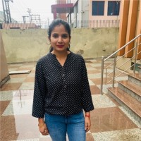
Ruby Adhana is listed as Sr. PCB Design engineer based in New Delhi, Delhi, India. AeroLeads shows a matched LinkedIn profile for Ruby Adhana.
Ruby Adhana previously worked as Senior Printed Circuit Board Designer at Techsb India Private Limited and Senior Printed Circuit Board Design Engineer at Huiseo Engineering Pvt Ltd. Ruby Adhana holds Diploma, Electrical, Electronics And Communications Engineering from Rajkiya Kanya Vidhalay.
Tool Expertise: ● Altium ● Pads ● Orcad ● Allegro ● Kicad ● CAM350● Strong working knowledge of orCAD schematic capture ,Allegro and PADS PCB design Tools including ● Proficient Technical skills using the cadence Allegro Design Toolset. ● Experience working with various system components such as LCD’s, Touch Panels,Microprocessor,Camera , Ethernet,ESP32,Pico w,RasberryPi,Arduino,Rock Hat,IoT Design,2G,4G,5G module, LoRaWan,LoRa etc. ● Experience in layout up to 6 layers Boards utilizing HDI Technology. ● Experience in routing as per rules. ● Experience designing PCBs for medium to high volume manufacturing. ● Generate, verify and validate Gerber data and perform design rule checks (DRC). I mostly exposed to following projects:- ● Bluetooth PCBs ● Wifi PCBs ● RF design PCBs ● MCU boards ● Prototyping ● Development boards ● Power design PCBs ● Pico ,Esp32,LoRa,Rock,Rasberry Pi and Arduino based design.My expertise:- ● PCB layout design ● Schematic capture ● Library creation , symbol and footprint ● Gerber generation ● Support for PCB manufacturing ● Support for complete design and development ● Support for components selection ● Creation of PCB Designs based on input( Schematics) from hardware team,Considering EMC guidelines and inputs from the project in order to achieve optimized design in terms of timing,cost,quality and manufacturability. Operate multimeter , vernier caliber.
A career timeline built from the work history available for this profile.
Noida, Uttar Pradesh, India
IoT designs,EPS32,Rock,Pico,Raspberry Pi,Arduino,2G,4G,5G,CM4,Graphics LCD,E-paper,TouchLCD GPS,Bluetooth and so on based designs……
Delhi, India
Battery management system 16 cells,BLDC ceiling fan

Delhi, India
Finger print reader,smart card reader

Delhi, India
Worked on Battery management system 16cells,Datalogger, smps 12V
Delhi, India
Worked on GPS, GSM, sensors, Stm32 series microcontrollers,stm8 series microcontrollers,Atmel chips.

Quick answers generated from the profile data available on this page.
Ruby Adhana is listed as Sr. PCB Design engineer.
Ruby Adhana is based in New Delhi, Delhi, India.
Ruby Adhana has worked for Techsb India Private Limited, Huiseo Engineering Pvt Ltd, Stj Electronic Pvt. Ltd, Lithion Power, and Deos Labs Private Limited.
You can use AeroLeads to view verified contact signals for Ruby Adhana, including work email, phone, and LinkedIn data when available.
Ruby Adhana holds Diploma, Electrical, Electronics And Communications Engineering from Rajkiya Kanya Vidhalay.
Search by job title, company, industry, location, and seniority. Export verified B2B contact data when you need it.
Start free trial Search contactsCheck these profiles if this is not the Ruby Adhana you were looking for.
View similar profiles