AeroLeads people directory · profile
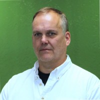
Sam Harkness Email & Phone Number
Distinguished Engineer
at
Western Digital
1 work email found
@intevac.com
LinkedIn matched
✓ Verified August 2026
4 data sources
Profile completeness 100%
Current company
Role
Distinguished Engineer
Location
Albany, California, United States
Who is Sam Harkness? Overview
A concise factual answer block for searchers comparing this professional profile.
Quick answer
Sam Harkness is listed as Distinguished Engineer at Western Digital, based in Albany, California, United States. AeroLeads shows a work email signal at intevac.com and a matched LinkedIn profile for Sam Harkness.
Sam Harkness previously worked as CTO, VP of Product Development & Technology at Intevac and Managing Director, Product Development & Technology at Intevac. Sam Harkness holds Ph.D., Material Science & Engineering from University Of Florida.
Company email context
Email format at Western Digital
This section adds company-level context without repeating Sam Harkness's masked contact details.
{first_initial}{last}@intevac.com
86% confidence
AeroLeads found 1 current-domain work email signal for Sam Harkness. Compare company email patterns before reaching out.
Profile bio
About Sam Harkness
Passionate about technology development and productization. My background in electronic materials, thin films, and capital equipment stretch across a myriad of industries including data storage, semiconductor, OLED, display, and solar, but common to them all is a long track record of utilizing the strength of my surroundings to lead, enhance or self-start many profitable projects. I believe in the stratagems of six sigma, FMEA and DOE in pursuit of productization and am experienced in setting up and executing in environments conducive to ideation and fast-fail. I have thick skin, I am not egotistical, and I enjoy learning as much as teaching. Finally, I thrive in team settings and believe that optimal outcomes come from being prepared at every meeting and convergence.Specialties: Roadmap vision, early stage technology development, equipment development, vendor liaison.
Listed skills include Thin Films, Sputtering, Nanotechnology, R&D, and 39 others.
Current workplace
Sam Harkness's current company
Company context helps verify the profile and gives searchers a useful next step.
12 roles · 31 years
Sam Harkness work experience
A career timeline built from the work history available for this profile.

Cto, Vp Of Product Development & Technology
Current
May 2022 - Present
Managing Director, Product Development & Technology
Aug 2021 - May 2022
Sr Director, Product Development & Technology
Aug 2020 - Aug 2021
Senior Director Of Technology
Jan 2019 - Aug 2020
Sr Mts
Oct 2018 - Jan 2019
Founder, Ceo
Hia Inc.
Conceived and created various PVD hardware products designed for mass production.
Sep 2014 - Aug 2020
Principal Technologist
Aug 2013 - Jun 2014
Device Scientist
Plextronics
Development of solution process OLED materials
Mar 2012 - Aug 2013
Sr Member Of The Technical Staff
Process design for thin film sputter platform. Development of new equipment for improved thin film quality.
Jan 2010 - Apr 2012

Senior Director
Advanced development of thin film nanostructures for magnetic recording media. Lead project for development novel photovoltaic concept.
Jun 1998 - Jan 2009
Applications Engineer
Product marketing for new capital equipment including turnkey process design, global customer interface, and applications trials execution.
1996 - 1998
~2 yrs
2 education records
Sam Harkness education
Ph.D., Material Science & Engineering
University Of Florida
B.S., Material Science & Engineering
University Of Florida
FAQ
Frequently asked questions about Sam Harkness
Quick answers generated from the profile data available on this page.
What company does Sam Harkness work for?
Sam Harkness works for Western Digital.
What is Sam Harkness's role at Western Digital?
Sam Harkness is listed as Distinguished Engineer at Western Digital.
What is Sam Harkness's email address?
AeroLeads has found 1 work email signal at @intevac.com for Sam Harkness at Western Digital.
Where is Sam Harkness based?
Sam Harkness is based in Albany, California, United States while working with Western Digital.
What companies has Sam Harkness worked for?
Sam Harkness has worked for Western Digital, Intevac, Hia Inc., Veeco Instruments, and Plextronics.
How can I contact Sam Harkness?
You can use AeroLeads to view verified contact signals for Sam Harkness at Western Digital, including work email, phone, and LinkedIn data when available.
What schools did Sam Harkness attend?
Sam Harkness holds Ph.D., Material Science & Engineering from University Of Florida.
What skills is Sam Harkness known for?
Sam Harkness is listed with skills including Thin Films, Sputtering, Nanotechnology, R&D, Characterization, Materials Science, Design Of Experiments, and Photovoltaics.
Find 750M verified contacts
Search by job title, company, industry, location, and seniority. Export verified B2B contact data when you need it.
Start free trial