
AeroLeads people directory · profile
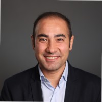
Hamed Sattari Email & Phone Number
Co-Founder and CEO
at
CCRAFT
1 work email found
@csem.ch
LinkedIn matched
✓ Verified July 2026
4 data sources
Profile completeness 100%
Current company
Role
Co-Founder and CEO
Location
Neuchâtel, Switzerland
Company size
Who is Hamed Sattari? Overview
A concise factual answer block for searchers comparing this professional profile.
Quick answer
Hamed Sattari is listed as Co-Founder and CEO at CCRAFT, a with 3 employees, based in Neuchâtel, Switzerland. AeroLeads shows a work email signal at csem.ch and a matched LinkedIn profile for Hamed Sattari.
Hamed Sattari previously worked as Technology Manager at Csem and Project Manager at Csem. Hamed Sattari holds Doctor Of Philosophy (Ph.D.), Photonics from University Of Tabriz.
Company email context
Email format at CCRAFT
This section adds company-level context without repeating Hamed Sattari's masked contact details.
{first}.{last}@csem.ch
86% confidence
AeroLeads found 1 current-domain work email signal for Hamed Sattari. Compare company email patterns before reaching out.
Profile bio
About Hamed Sattari
At CSEM, my role as Technology Manager encompasses leading a team of experts in advanced photonic chip design and ensuring the highest standards in manufacturing and quality assurance. We've established strong B2B connections, contributing to robust R&D processes and shared success. My background in PIC and MEMS technologies and project management have been instrumental in securing substantial funding, enhancing project execution, and fostering international collaborations.With a focus on strategic development within the PIC platforms, my work also involves engaging with over 40 partners worldwide, which has cultivated a strong network that supports both academic and industrial advancements. My technical expertise in PICs, coupled with a strategic approach to product development and business planning, continues to drive innovation in applications ranging from telecom to quantum technology.
Listed skills include Photonics, Physics, Matlab, Optics, and 16 others.
Current workplace
Hamed Sattari's current company
Company context helps verify the profile and gives searchers a useful next step.
Ccraft
9 roles
Hamed Sattari work experience
A career timeline built from the work history available for this profile.

Co-Founder And Ceo

Technology Manager
- Coordinating a team of 20 experts and engineers, overseeing photonic chip design, manufacturing, and quality assurance.- Playing a key role in defining internal strategic development threads for the TFLN PIC Platform.- Cultivate direct relationships with 40+ end users and partners worldwide to ensure robust B2B connections, fostering a healthy R&D process and mutual success.- Actively presenting and networking within the PIC community to discern and address the needs of both academia and industry stakeholders.
Project Manager
- Key role in securing 10 M€ in public and industrial funds for various projects.-Managing and executing industrial and public projects involving local and international stakeholders.
Sep 2022 - Jan 2024
Senior Research And Development Engineer
We functionalize PICs for a variety of applications, just a few to mention, such as the LNOI platform for telecom and quantum technology, or SiN for various sensing scenarios. We foster substantial microfabrication techniques for process development, and with the support of our expertise in the design, simulation, and characterization of PICs, first, we provide disruptive solutions for the emerging needs, and second, we support the industry with innovative offerings.
Mar 2020 - Sep 2022

Researcher - Silicon Photonics - Mems
Active on two main projects on Optical MEMS:1) Mems-based zerO-power Reconfigurable PHotonic ICs (MORPHIC Project):In MORPHIC (H2020 funded), we enhance an established Silicon Photonics platform with MEMS actuators so photonic circuits can be programmed for a variety of optical functions with built-in redundancy and resilience. We fulfill the design of individual components, floorplan preparation and tape-out of the photonic chip, post-processing of the wafers, and characterization of the chip. 2) Bistable Silicon Photonic MEMS Switches:In this project, we exploit mechanical bistability for silicon photonic MEMS switches. This mechanism can lead to an overall drastically reduced power consumption for the optical switch. We developed a compact bistable photonic switch architecture using advanced FEM and FDTD simulation tools and successfully demonstrated the bistability concept. We also take advantage of a Stepper machine for photolithography which enables high throughput and fast fabrication processes with outstanding precision.
Sep 2017 - Dec 2020
Researcher
Swiss Government Excellence Scholarship Award-> Diamond Photonics (Design, Simulation, Microscopy)Camlin Technologies Switzerland-> High Contrast Gratings for VECSELs
Sep 2016 - Sep 2017
Research And Development Engineer
As a part of the R&D team, I was involved in the design and simulation tasks which were focused on the Metasurfaces, Double Negative Materials, and Extraordinary Transmissive structures. I developed a design for plasmonic Antennas for light steering applications.https://www.osapublishing.org/oe/abstract.cfm?uri=oe-25-25-30827
May 2016 - Sep 2016
Research Fellow
Supervising projects in Quantum Optics and Integrated Photonics
Dec 2014 - Feb 2016
3 education records
Hamed Sattari education
Doctor Of Philosophy (Ph.D.), Photonics
University Of Tabriz
Master'S Degree, Photonics
University Of Tabriz
Bachelor'S Degree, Atomic/Molecular Physics
University Of Tabriz
FAQ
Frequently asked questions about Hamed Sattari
Quick answers generated from the profile data available on this page.
What company does Hamed Sattari work for?
Hamed Sattari works for CCRAFT.
What is Hamed Sattari's role at CCRAFT?
Hamed Sattari is listed as Co-Founder and CEO at CCRAFT.
What is Hamed Sattari's email address?
AeroLeads has found 1 work email signal at @csem.ch for Hamed Sattari at CCRAFT.
Where is Hamed Sattari based?
Hamed Sattari is based in Neuchâtel, Switzerland while working with CCRAFT.
What companies has Hamed Sattari worked for?
Hamed Sattari has worked for Ccraft, Csem, Epfl (École Polytechnique Fédérale De Lausanne), Nanotam - Bilkent University Nanotechnology Research Center, and University Of Tabriz.
How can I contact Hamed Sattari?
You can use AeroLeads to view verified contact signals for Hamed Sattari at CCRAFT, including work email, phone, and LinkedIn data when available.
What schools did Hamed Sattari attend?
Hamed Sattari holds Doctor Of Philosophy (Ph.D.), Photonics from University Of Tabriz.
What skills is Hamed Sattari known for?
Hamed Sattari is listed with skills including Photonics, Physics, Matlab, Optics, Research, Nanotechnology, Nonlinear Optics, and Laser Physics.
Find 750M verified contacts
Search by job title, company, industry, location, and seniority. Export verified B2B contact data when you need it.
Start free trial