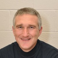
Senior Physical Design Engineer
Current
Oct 2018 - Present
Please complete the CAPTCHA to continue

@ibm.com
✓
LinkedIn matched
A concise factual answer block for searchers comparing this professional profile.
Scott Warnock is listed as Senior Physical Design Engineer at IBM, a with 512090 employees, based in Portland, Oregon, United States. AeroLeads shows a work email signal at ibm.com and a matched LinkedIn profile for Scott Warnock.
Scott Warnock previously worked as Physical Design Engineer at Computer Task Group and VLSI Design Engineer at Ibm. Scott Warnock holds Bachelor Of Applied Science (B.A.Sc.), Electrical And Electronics Engineering from University Of Ottawa.
This section adds company-level context without repeating Scott Warnock's masked contact details.
AeroLeads found 2 current-domain work email signals for Scott Warnock. Compare company email patterns before reaching out.
VLSI physical design for IBM's Systems and Technology Group (STG) microprocessor division.Skills include: custom circuit design, RLM design, timing closure, physical layout and DRC and LVS resolution, DFT concepts, vhdl, perl and unix scripting, cadence skill programming and database access, emacs
Listed skills include Circuit Design, Vlsi, Vhdl, Microprocessors, and 14 others.
Company context helps verify the profile and gives searchers a useful next step.
A career timeline built from the work history available for this profile.

Austin, Tx
2008/7 – 2014/3Clib (common library) lead for P and Z series. Support and delivery of common IP for IBM's various processor groups. 2005/5 - 2008/7IBM P series microprocessor circuit design - LSU circuit design, register file team, library latch and LCB design2001/8 – 2005/5; Austin, TX: IBM Microelectronics Division STI (Sony-Toshiba-IBM - Playstation 3 chip)Circuit design, unit floorplanning, critical path analysis, physical, and physical design methodology. Library support.1998/7 – 2001/8, Austin, TX:IBM Server Group – custom circuit designer for IBM’s gigahertz (GP, Power4) chip. Responsible for all stages of design of several custom, semi-custom, macros, synthesis and build of several RLM’s.1996/11- 1998/7, Watson Research, Yorktown Heights, NY3-4 months intensive VLSI circuit design training, then circuit design for Pulsar (AS400) chip

Various microprocessor and DSP based designs (board level) for one of Canada’s leading high tech companies and the world leader in flight simulators. Responsible for all stages of design from conception, design, test software and manufacturing support. Designs included:- A real time image-remapper to correct for projection optics in a head-mounted display.- A vector video to raster video converter to display radar images on a raster display.- Research and support for an HDTV helmet mounted display system.- Embedded microprocessor based serial controllers for various avionics interfaces.
Ottawa, Canada Area
Responsible for a wide range of engineering duties typical of a small company including production supervision, devising test strategies, environmental and acceptance testing and field work. Planned and gave a two week maintenance training course for Transport Canada technicians.
Other employees you can reach at ibm.com. View company contacts for 512090 employees →
 Gerardo Parra
Colleague at IbmBogota, D.C., Capital District, Colombia
View →
DD
Gerardo Parra
Colleague at IbmBogota, D.C., Capital District, Colombia
View →
DD
 Denis Doherty
Colleague at IbmUnited Kingdom
View →
KS
Denis Doherty
Colleague at IbmUnited Kingdom
View →
KS
 K Surender
Colleague at IbmHyderabad, Telangana, India
View →
AS
K Surender
Colleague at IbmHyderabad, Telangana, India
View →
AS
 Akash Shukla
Colleague at IbmBengaluru, Karnataka, India
View →
XZ
Akash Shukla
Colleague at IbmBengaluru, Karnataka, India
View →
XZ
 Xinyu Zhao
Colleague at IbmYokohama, Kanagawa, Japan
View →
GD
Xinyu Zhao
Colleague at IbmYokohama, Kanagawa, Japan
View →
GD
 Gaëlle Dussutour-Tan
Colleague at IbmGreater Paris Metropolitan Region, France
View →
SK
Gaëlle Dussutour-Tan
Colleague at IbmGreater Paris Metropolitan Region, France
View →
SK
 Suresh Kanal
Colleague at IbmFront Royal, Virginia, United States
View →
JL
Suresh Kanal
Colleague at IbmFront Royal, Virginia, United States
View →
JL
 Juan Luis Medel
Colleague at IbmGuadalajara, Jalisco, Mexico
View →
HM
Juan Luis Medel
Colleague at IbmGuadalajara, Jalisco, Mexico
View →
HM
 Hadel Magdy
Colleague at IbmEl Sheikh Zaid, Al Jizah, Egypt
View →
VP
Hadel Magdy
Colleague at IbmEl Sheikh Zaid, Al Jizah, Egypt
View →
VP
 Vito Pagliaccio
Colleague at IbmMilan, Lombardy, Italy
View →
Vito Pagliaccio
Colleague at IbmMilan, Lombardy, Italy
View →

Quick answers generated from the profile data available on this page.
Scott Warnock works for IBM.
Scott Warnock is listed as Senior Physical Design Engineer at IBM.
AeroLeads has found 2 work email signals at @ibm.com for Scott Warnock at IBM.
Scott Warnock is based in Portland, Oregon, United States while working with IBM.
Scott Warnock has worked for Ibm, Computer Task Group, Cae, and Audor Communications Inc.
Scott Warnock's colleagues at IBM include Gerardo Parra, Denis Doherty, K Surender, Akash Shukla, and Xinyu Zhao.
You can use AeroLeads to view verified contact signals for Scott Warnock at IBM, including work email, phone, and LinkedIn data when available.
Scott Warnock holds Bachelor Of Applied Science (B.A.Sc.), Electrical And Electronics Engineering from University Of Ottawa.
Scott Warnock is listed with skills including Circuit Design, Vlsi, Vhdl, Microprocessors, Perl, Physical Design, Asic, and Semiconductors.
Search by job title, company, industry, location, and seniority. Export verified B2B contact data when you need it.
Start free trial Search contactsCheck these profiles if this is not the Scott Warnock you were looking for.