Professional Retiree
Current
Self-Employed
Jan 2018 - Present
Please complete the CAPTCHA to continue
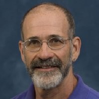
@agilent.com
✓
LinkedIn matched
A concise factual answer block for searchers comparing this professional profile.
Jeff Rosner is listed as Professional Retiree at Self-employed, based in San Francisco Bay Area, United States. AeroLeads shows a work email signal at agilent.com and a matched LinkedIn profile for Jeff Rosner.
Jeff Rosner previously worked as Co-founder at Floragraph Llc and Private Biotechnology Consultant at Sjr Consulting. Jeff Rosner holds Ph.D., Materials Science from Stanford University.
This section adds company-level context without repeating Jeff Rosner's masked contact details.
AeroLeads found 1 current-domain work email signal for Jeff Rosner. Compare company email patterns before reaching out.
Jeff is a Ph.D. level professional currently in an executive position with a highly diverse background in science, technology and business fundamentals. He has demonstrated his ability to thrive in a variety of environments ranging from the highly focused product development paradigm to scenarios that include a high degree of uncertainty and risk. This includes a consistent track record of startup and commercialization of new technologies and business footprints within multi-national, Fortune 500 technology companies, as well as a history of providing leadership and focus to create high performance teams. Personal assets include:- Extensive experience in research and development: over two decades of participation at all organizational levels including product development engineer and project management, distinguished senior research scientist, R&D manager, incubation manager in an intrapeneurial setting.- Leadership and contribution in research, strategy determination, product development and operational management across a broad array of business footprints including analytical instrumentation, compound semiconductor and silicon based devices and integrated circuits, manufacturing inspection equipment, nanoscale measurement instruments, microfluidics and genomic microarrays.- Skill at surveying and distilling technology landscapes, selecting focus areas and sourcing appropriate technology acquisitions, including product strategy and integration activities. - Scientific contribution and innovation as evidenced by more than 50 scientific journal articles and 15 issued US patents (and associated foreign filings).
Listed skills include R&D, Nanotechnology, Lifesciences, Commercialization, and 27 others.
Company context helps verify the profile and gives searchers a useful next step.
A career timeline built from the work history available for this profile.
Palo Alto, Ca

San Francisco Bay Area
Floragraph is an early-stage company created to enable Personal Microbiome Monitoring in the context of the Quantified Self (QS) movement. Our goal is to develop and provide an at-home consumer solution that allows individuals to monitor the quantity and diversity of their gut microbiome. In combination with annotation (health, diet,...), this will enable us to build an online, data-driven presence that assembles the annotation and data (linking the solution through mobile phones) for… Show more Floragraph is an early-stage company created to enable Personal Microbiome Monitoring in the context of the Quantified Self (QS) movement. Our goal is to develop and provide an at-home consumer solution that allows individuals to monitor the quantity and diversity of their gut microbiome. In combination with annotation (health, diet,...), this will enable us to build an online, data-driven presence that assembles the annotation and data (linking the solution through mobile phones) for community, science, and policy applications. Show less
Palo Alto, Ca
Broad technical and market background - Genomic analytical solutions - Materials science and semiconductors - Complex systems integrationVenture investing and M&A support - Technical and IP diligence - Market and strategic analysis

S. San Francisco, California
Chief Technology Officer and strategy for the former Applied Biosystems, Inc franchise. Drive incubation and open innovation practices to create investment options for next generation genetic analysis science and technology. Engage academic and entrepreneur community to accelerate commercialization of new approaches to genetic analysis. Sourcing and diligence of acquisition targets. Synthesize and validate strategic options for annual planning cycle.
Foster City, Ca
Accountable for strategy and execution of technology and product roadmap for all realtime PCR and capillary electrophoresis systems and consumables including digital PCR. $65M budget and ~250 R&D staff in a global organization. Chair of Corporate Science Council.
Eugene, Oregon Area
Managed a team of researchers working on surface chemistry and nanostructured materials related to development of single-molecule genomic sequencing technology.

Director of Technology and Strategy for startup business within Agilent. Responsible for definition of growth strategy through internal R&D activities, licensing and technology acquisition deal sourcing and diligence, and equity investments up to and including acquisitions. Coordinate R&D for existing $150M business and orchestrate intra-corporate collaborative projects to create additional value. Primary technology focus is nanotechnology with an emphasis on microscopy and spectroscopy. Market… Show more Director of Technology and Strategy for startup business within Agilent. Responsible for definition of growth strategy through internal R&D activities, licensing and technology acquisition deal sourcing and diligence, and equity investments up to and including acquisitions. Coordinate R&D for existing $150M business and orchestrate intra-corporate collaborative projects to create additional value. Primary technology focus is nanotechnology with an emphasis on microscopy and spectroscopy. Market emphasis is on adding additional product categories to Life Science offerings. Show less
2005 – Agilent Corporate – Incubation manager Manage small team incubating new business within a larger “New Business Creation” organization. 2003-2005 – Agilent Laboratories – Senior Scientist Senior scientist in new business development role. Explore opportunities for green field research opportunities. Identify promising new business areas for Agilent; work with Corporate Development and internal Agilent Ventures organization to locate and promote strategic investments in… Show more 2005 – Agilent Corporate – Incubation manager Manage small team incubating new business within a larger “New Business Creation” organization. 2003-2005 – Agilent Laboratories – Senior Scientist Senior scientist in new business development role. Explore opportunities for green field research opportunities. Identify promising new business areas for Agilent; work with Corporate Development and internal Agilent Ventures organization to locate and promote strategic investments in external technology sources. Act as initial principal investigator for new research activities at Labs. Show less
Agilent Laboratories (HP Labs before 1999), Palo Alto, CA – R&D Manager Manager and scientific leader of materials research group involved in a variety of programs in collaboration with other HP Labs entities and product divisions. Charter to resolve materials processing issues critical to current and future HP business by integrating analytical materials science with in-depth understanding of materials properties and processing requirements. Group project areas included epitaxial… Show more Agilent Laboratories (HP Labs before 1999), Palo Alto, CA – R&D Manager Manager and scientific leader of materials research group involved in a variety of programs in collaboration with other HP Labs entities and product divisions. Charter to resolve materials processing issues critical to current and future HP business by integrating analytical materials science with in-depth understanding of materials properties and processing requirements. Group project areas included epitaxial semiconductor devices, CMOS ICs, Light-Emitting-Diodes (LEDs), solder metallurgy, surface modification for life science applications, micro-fluidic consumables, x-ray imaging. Show less

Hewlett-Packard Integrated Circuit Business Div., Palo Alto, CA – R&D / Yield ManagerManagement of a cross-disciplinary team of engineers working on multi-level interconnects for high performance integrated circuit products. Responsible for institution of Statistical Quality Control methods to drive fast ramp to high-yield for new processes in multiple facilities worldwide. Specification and introduction of failure analysis techniques and equipment.
Palo Alto, Ca
Hewlett-Packard Laboratories, Palo Alto, CA - Senior Member, Technical StaffMember of materials research group involved in electronic materials investigations, primarily in the areas of hetero-epitaxial crystal growth for light-emitting diodes (LEDs), and thin metal films used in integrated circuit fabrication. Responsible for Rutherford backscattering spectrometry/ion channeling and transmission and scanning electron microscopy technology, liaisons with other thin film analytical… Show more Hewlett-Packard Laboratories, Palo Alto, CA - Senior Member, Technical StaffMember of materials research group involved in electronic materials investigations, primarily in the areas of hetero-epitaxial crystal growth for light-emitting diodes (LEDs), and thin metal films used in integrated circuit fabrication. Responsible for Rutherford backscattering spectrometry/ion channeling and transmission and scanning electron microscopy technology, liaisons with other thin film analytical techniques (Auger, SIMS, optical spectroscopy, X-ray analysis), and experimental coordination of materials issues in thin film development. Show less
Hewlett-Packard Scientific Instrument Div., Palo Alto, CA - Design Engineer and Project ManagerSystem and component design of analytical equipment for organic chemistry research, primarily in the area of combined gas chromatography & quadrupole mass spectrometry systems for multi-component analysis. Responsible for both electronic measurement and mechanical R&D, including ion optical design. Developed liquid introduction system to enable liquid chromatography (LC) integration (LC/MS).… Show more Hewlett-Packard Scientific Instrument Div., Palo Alto, CA - Design Engineer and Project ManagerSystem and component design of analytical equipment for organic chemistry research, primarily in the area of combined gas chromatography & quadrupole mass spectrometry systems for multi-component analysis. Responsible for both electronic measurement and mechanical R&D, including ion optical design. Developed liquid introduction system to enable liquid chromatography (LC) integration (LC/MS). Extended mass range of quadrupole mass filter to 2000 daltons in product, 3000 daltons in laboratory environment. Show less

ISS Sperry Univac, Mountain View, CA - Staff EngineerDesigned and developed head positioning servo equipment for large "Winchester type" disc memory systems, including design and test for final production release. Developed patented servo feedback pattern and microprocessor controlled in situ test capability for use in same product. Developed manufacturing version of servo track recording system for production; developed ultra-precise head positioning and read/write test station for… Show more ISS Sperry Univac, Mountain View, CA - Staff EngineerDesigned and developed head positioning servo equipment for large "Winchester type" disc memory systems, including design and test for final production release. Developed patented servo feedback pattern and microprocessor controlled in situ test capability for use in same product. Developed manufacturing version of servo track recording system for production; developed ultra-precise head positioning and read/write test station for advanced thin-film head/disc development. Show less

NASA Ames, Moffett Field, CA - Contract engineerDesigned acoustic surveillance equipment for Navy system; including hydrophone design, data acquisition subsystem, and communications electronics.

Medical Information Technology, Cambridge, MA - Principal engineer Start-up operation; designed computer interfaces to laboratory equipment and custom peripherals.

Developed and analyzed interfaces associated with heteroepitaxial crystal growth in compound semiconductor systems.

Signals and Systems concentration; developed pre-processing techniques for optimization of digital audio.
Quick answers generated from the profile data available on this page.
Jeff Rosner works for Self-employed.
Jeff Rosner is listed as Professional Retiree at Self-employed.
AeroLeads has found 1 work email signal at @agilent.com for Jeff Rosner at Self-employed.
Jeff Rosner is based in San Francisco Bay Area, United States while working with Self-employed.
Jeff Rosner has worked for Self-Employed, Floragraph Llc, Sjr Consulting, Life Technologies, and Agilent Technologies.
You can use AeroLeads to view verified contact signals for Jeff Rosner at Self-employed, including work email, phone, and LinkedIn data when available.
Jeff Rosner holds Ph.D., Materials Science from Stanford University.
Jeff Rosner is listed with skills including R&D, Nanotechnology, Lifesciences, Commercialization, Spectroscopy, Product Development, Genomics, and Biotechnology.
Search by job title, company, industry, location, and seniority. Export verified B2B contact data when you need it.
Start free trial Search contactsCheck these profiles if this is not the Jeff Rosner you were looking for.