Sep 2024 - Present
Please complete the CAPTCHA to continue
@cornell.edu
✓
LinkedIn matched
A concise factual answer block for searchers comparing this professional profile.
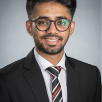
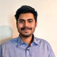
Sudarshan Sundar is listed as Yield Enhancement @ Micron at Micron Technology, a with 20793 employees, based in Boise, Idaho, United States. AeroLeads shows a work email signal at cornell.edu and a matched LinkedIn profile for Sudarshan Sundar.
Sudarshan Sundar previously worked as Yield Enhancement at Micron Technology and Product Development Engineer at Intel Corporation. Sudarshan Sundar holds Master Of Science - Ms, Materials Science And Engineering, 3.85/4 from Cornell University.
This section adds company-level context without repeating Sudarshan Sundar's masked contact details.
AeroLeads found 1 current-domain work email signal for Sudarshan Sundar. Compare company email patterns before reaching out.
Semiconductor professional with experience in Process Engineering, Yield Technology and Product Development
Listed skills include Microsoft Office, Nanotechnology, Matlab, Cad, and 32 others.
Company context helps verify the profile and gives searchers a useful next step.
A career timeline built from the work history available for this profile.

Portland, Oregon Metropolitan Area
Global External Manufacturing & Sourcing
Hillsboro, Oregon, United States
Technology Development Low Yield Analysis Engineer for next gen Intel transistors
Hillsboro, Oregon, United States
TD Module &Integration Yield Engineer - Etch
Ithaca, New York Area
Masters Thesis (September 2018 - Present)High-Throughput Synthesis and Characterization of Metastable Materials:•Advanced high-throughput metrology & reliability of dielectric thin films deposited by Physical Vapor Deposition• Designed Photomask and developed liftoff process using photolithography for Platinum contact pads for probe measurements• Implemented Statistical process control to eliminate pinhole defects during capacitance cell device nanofabrication• Devised a mechanism for mapping metastable phases by validating with Spectroscopy, Optical Imaging and XRD

San Francisco Bay Area
• Improved SoC die attach assembly by implementing Statistical Process Control and Optical Metrology inspections• Resolved the reworkability of PCB Bonding film lamination in Flip-chip BGA packaging with Design of Experiments• Optimized MEMS probe spring metallurgy through SEM grain size estimation to withstand a million-lifecycle bend testing• Won the Most Innovative Poster Presentation Award during 'FormFactor Inc. Interns Poster Session Event 2019'.

Ithaca, New York Area
Hall Effect and Van der Pauw measurement:- Estimated Sheet Resistance, Sheet Carrier density, Electron mobility of Silicon wafer using 4 point measurement.- 'R' values were measured with 4*4 combinations of 'V' and 'I' to estimate the "Rs" value iteratively.- Hall effect measurement value of the sample is then calculated in the presence of a magnetic field.Contrast Curve Measurement using Photolithography:- Developed photoresist and inspected the resist thickness using Filmetrics, which measures filmthickness based on light interference.- Si wafer is coated with PR, soft baked and exposed methodically under UV lamp of determined intensity. - The curve is estimated with a semi-logarithmic plot of thickness Vs UV dosage. Hence, the slope is calculated.Fabrication and Characterization of MoS2 Thin Film Transistor :- Implemented dry transfer of MoS2 on PDMS stamp with the pre-patterned electrode using Photolithography- Devised 4-probe and output I-V characteristics (ID-VG), to obtain the ON-resistance of the FET with and without light

Pune Area, India
Metallurgy Laboratory, Aluminum & Cast Iron Foundry:• Supervised the laboratory operations of Spectrometry and Mechanical testing as per ISO/TS 16949:2009 standards.• Inspected supplier materials quality during vendor visits to meet the World Class Quality (WCQ) standards.• Performed Failure analysis of rejected castings and implemented Action plans for defect control.• Implemented Six Sigma DMAIC Root Cause analysis using SPC, FMEA.• Achieved a lower castings rejection rate of Aluminum 3-ltr engine blocks from 38 to 3 percent towards March 2018, resulting in savings upwards of USD 80,000 per annum.

Chennai Area, India
Advanced High Strength Steels in the Automotive Industry:• Documented the novel heat treatment approaches on Automotive Steels as per the AHSS guidelines V5.0.• Designed the heat treatment cycle for Quenched partitioning treatment in the Gleeble 3800-GTC Thermo Mechanical Simulator (TMS).• Prepared study material on Automotive steels and their processing methods.

India
Mechanical behavior of Cu-Zn-Pb alloys upon Annealing and Severe Plastic Deformation : • Brass alloys of varying Pb concentrations were subjected to Annealing, followed by Mechanical testing and Route-A ECAP process.• Significant improvement in ductility was achieved but failure to undergo ECAP process was reported• Lead (Pb) segregation was identified upon EDS analysis using a HITACHI S-3000H electron microscope.• A technical paper on this study was presented at the 12th IRF International Conference at Goa,India (Sep 2017).

Singapore
(Singapore Pre-Graduate Award Fellowship, 2016)• Worked in Class 100 (ISO class 5) cleanroom.• Achieved controlled Molecular Beam Epitaxial growth of Ag thin film of 100 nm thickness at a rate of 2 nm/s on mica substrate by controlling process parameters of electron beam evaporation chamber.• Estimated the dielectric properties upon optical characterization using Ellipsometry and Spectrophotometry analysis in the UV-VIS wavelength range.• Characterized stable uniform epitaxial growth by electron microscope studies (SEM)

Polymer Nanocomposite Multiscale Modeling :• Synthesized Polydimethylsiloxane (PDMS) with Graphene Nanosheet reinforcement by Physical blend method.• Characterized stable dispersion interface using Quanta FIB Dual Beam SEM.• Simulated interfacial stress contours of tensile response in ABAQUS using the Mean field homogenization method.• Achieved 45 percent improvement in Elastic moduli upon dispersion

Testing of Advanced Composite materials :• Studied chemical analysis of polymer-clay composites using ICP optical emission spectroscopy, BrukerNMR and FTIR.• Additionally trained in failure analysis methods using bend test and torsion testing
Other employees you can reach at micron.com. View company contacts for 20793 employees →
 Mark Helm
Colleague at Micron TechnologySan Jose, California, United States
View →
CC
Mark Helm
Colleague at Micron TechnologySan Jose, California, United States
View →
CC
 Chris C.
Colleague at Micron TechnologyBoise, Idaho, United States
View →
YT
Chris C.
Colleague at Micron TechnologyBoise, Idaho, United States
View →
YT
 Yi Tong Lin
Colleague at Micron TechnologyTaoyuan City, Taiwan, Province Of China
View →
SJ
Yi Tong Lin
Colleague at Micron TechnologyTaoyuan City, Taiwan, Province Of China
View →
SJ
 Sunidhi Jain
Colleague at Micron TechnologySanand, Gujarat, India
View →
RS
Sunidhi Jain
Colleague at Micron TechnologySanand, Gujarat, India
View →
RS
 Roger Seow
Colleague at Micron TechnologySingapore
View →
DS
Roger Seow
Colleague at Micron TechnologySingapore
View →
DS
 Dereck Stertz
Colleague at Micron TechnologyBroomfield, Colorado, United States
View →
PG
Dereck Stertz
Colleague at Micron TechnologyBroomfield, Colorado, United States
View →
PG
 Parth Gandani
Colleague at Micron TechnologyRoxbury Crossing, Massachusetts, United States
View →
HL
Parth Gandani
Colleague at Micron TechnologyRoxbury Crossing, Massachusetts, United States
View →
HL
 Hunna Liu
Colleague at Micron TechnologyFalls Church, Virginia, United States
View →
GC
Hunna Liu
Colleague at Micron TechnologyFalls Church, Virginia, United States
View →
GC
 Gabriel Cavazos
Colleague at Micron TechnologyBoise Metropolitan Area, United States
View →
GH
Gabriel Cavazos
Colleague at Micron TechnologyBoise Metropolitan Area, United States
View →
GH
 Garrett Harwell
Colleague at Micron TechnologyMeridian, Idaho, United States
View →
Garrett Harwell
Colleague at Micron TechnologyMeridian, Idaho, United States
View →
Activities and Societies:Spring 2019 Teaching Assistant: MSE 5150: Structures and Materials for Sustainable Energy Systems.
Quick answers generated from the profile data available on this page.
Sudarshan Sundar works for Micron Technology.
Sudarshan Sundar is listed as Yield Enhancement @ Micron at Micron Technology.
AeroLeads has found 1 work email signal at @cornell.edu for Sudarshan Sundar at Micron Technology.
Sudarshan Sundar is based in Boise, Idaho, United States while working with Micron Technology.
Sudarshan Sundar has worked for Micron Technology, Intel Corporation, Cornell University, Formfactor Inc., and Cornell Nanoscale Science & Technology Facility.
Sudarshan Sundar's colleagues at Micron Technology include Mark Helm, Chris C., Yi Tong Lin, Sunidhi Jain, and Roger Seow.
You can use AeroLeads to view verified contact signals for Sudarshan Sundar at Micron Technology, including work email, phone, and LinkedIn data when available.
Sudarshan Sundar holds Master Of Science - Ms, Materials Science And Engineering, 3.85/4 from Cornell University.
Sudarshan Sundar is listed with skills including Microsoft Office, Nanotechnology, Matlab, Cad, Deform, Teamwork, Imagej, and Vic 2D.
Search by job title, company, industry, location, and seniority. Export verified B2B contact data when you need it.
Start free trial Search contactsCheck these profiles if this is not the Sudarshan Sundar you were looking for.