
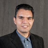
AeroLeads people directory · profile
Babak Talebanpour Email & Phone Number
Lead Semiconductor Packaging Engineer
at
Quantinuum
2 work emails found
@starkey.com
LinkedIn matched
✓ Verified Jul 2026
4 data sources
Profile completeness 100%
Current company
Role
Lead Semiconductor Packaging Engineer
Location
Greater Minneapolis-St. Paul Area, United States
Company size
Who is Babak Talebanpour? Overview
A concise factual answer block for searchers comparing this professional profile.
Quick answer
Babak Talebanpour is listed as Lead Semiconductor Packaging Engineer at Quantinuum, a with 558 employees, based in Greater Minneapolis-St. Paul Area, United States. AeroLeads shows a work email signal at starkey.com and a matched LinkedIn profile for Babak Talebanpour.
Babak Talebanpour previously worked as Principal Microelectronic Packaging Engineer at Starkey Hearing and Principal Microelectronic Packaging Engineer at Starkey Hearing. Babak Talebanpour holds Doctor Of Philosophy (Ph.D.), Materials Science And Engineering/Mechanical Engineering, 3.88 from Washington State University.
Company email context
Email format at Quantinuum
This section adds company-level context without repeating Babak Talebanpour's masked contact details.
{first}_{last}@starkey.com
89% confidence
AeroLeads found 2 current-domain work email signals for Babak Talebanpour. Compare company email patterns before reaching out.
Profile bio
About Babak Talebanpour
• Extensive experience in design, simulation, prototyping, fabrication, characterization and reliability of microelectronic circuits, and multi-chip modules. • Proficient in bridging disciplines such as Electrical, RF, Materials, and Mechanical Engineering. • Demonstrates exceptional written and verbal communication skills. • Possesses strong coordination abilities and adept at managing multiple projects and priorities to meet deadlines.
Listed skills include Microsoft Office, Research, C++, Matlab, and 32 others.
Current workplace
Babak Talebanpour's current company
Company context helps verify the profile and gives searchers a useful next step.
Quantinuum
8 roles
Babak Talebanpour work experience
A career timeline built from the work history available for this profile.

Principal Microelectronic Packaging Engineer

Principal Microelectronic Packaging Engineer
Sr. Microelectronic Packaging Engineer Ii
Dec 2019 - Jul 2024
Sr. Microelectronic Packaging Engineer I
I am responsible for advancing microelectronic packaging technology through Ideation, modern Microelectronic Design, Material Selection, Technology Scanning, Competitive Benchmarking, and Finite Element Modeling. I pursue the newest packaging technology, carrying out fitness for use studies, driving down microelectronic package size, improving package functionality and ease of manufacturability.Responsibilities:• Led the development, ie. definition, design, manufacturing, design verification, reliability verification, and qualification, of multi-chip modules. • Developed microelectronic packages with advanced technologies including; Embedded SoC, Flip chip on flex, Folded Flex packages, Package on Package, Wirebond die stack, and 3D stacking.• Led packaging pathfinding, established relationship with suppliers and subcontractors to develop roadmaps and develop packages with new technologies eg. FOWLP and TSVs.• Ran decision analyses, DFMEAs, and risk registers.• Designed, and implemented DOEs for tens of projects. • Completed numerous comprehensive Root Cause Analyses.• Collaborated with OSATs on failure analyses and corrective actions.• Participated in process development for new microelectronic designs.• Performed Finite Element Analyses on microelectronic packaging concepts, and production packages to evaluate Thermo-mechanical robustness.• Performed exhaustive Technology Scanning and benchmarking of microelectronic packaging industries. Monitored packaging roadmaps and trends eg. chiplets, interposers, heterogeneous integration.
Aug 2015 - Dec 2019

Multi-Physics Laboratories Manager
• Responsible for $1 M equipment operations across three laboratories. • Installed new equipment (white light interferometer) and relocated existing equipment (scanning electron microscope and dynamic mechanical analyzer).• Trained 15 graduate students on equipment use, research techniques, and laboratory policies.• Oversaw inventory and supply for laboratories, including scheduling consumable orders.
Aug 2013 - Aug 2015
Graduate Research Assistant
Fracture Behavior Characterization of Simulated Microbumps • Implemented SolidWorks to build CAD model of sample/experimental setup.• Fabricated over 200 simulated microbump samples (20μm thick) with various morphologies by analytically modeling the kinetics of intermetallic growth.• Performed fracture tests, analyzed data, calculated percent of different fracture modes.• Devised and produced the world’s first fracture mechanism map for simulated microbumps. • Increased the toughness of the solder joints at least 25% by redesigning the joints’ configuration.• Prepared multiple reports and presentations for Semiconductor Research Corporation.• Presented project accomplishments in Semiconductor Research Corporation annual meeting (June 2014).Modelling Creep of Solder Joints at Simulated Service Conditions • Fabricated solder joints with microstructures simulating samples in storage and at service.• Performed indentation 350 creep tests, analyzed data, and measured characteristic creep parameters.• Developed a new composite model and validated the model with experimental data.• Achieved approximately 5% more accurate predictions with the new model compared to previous models.• Prepared 6 quarterly reports, 1 midterm report and 1 final report, presented to Strategic Environmental Research and Development Program.Characterizing/Modelling Microstructural Evolution in Solders During Thermomechanical Excursions• Implemented multiple microstructural characterization techniques to measure the key microstructure parameters as the joints were subjected to thermomechanical excursions.• Created a prediction graph to integrate all data into one source.
Feb 2011 - Aug 2015
Assistant Lecturer
• Taught 25 graduate students in Advanced Materials Science• Assisted primary instructor in educating 100 undergraduate students in Introduction to Materials Science
Aug 2013 - May 2014
3 education records
Babak Talebanpour education
Doctor Of Philosophy (Ph.D.), Materials Science And Engineering/Mechanical Engineering, 3.88

Master Of Science (M.S.), Mechanical/Materials Engineering
Bachelor Of Science (B.S.), Materials Engineering
FAQ
Frequently asked questions about Babak Talebanpour
Quick answers generated from the profile data available on this page.
What company does Babak Talebanpour work for?
Babak Talebanpour works for Quantinuum.
What is Babak Talebanpour's role at Quantinuum?
Babak Talebanpour is listed as Lead Semiconductor Packaging Engineer at Quantinuum.
What is Babak Talebanpour's email address?
AeroLeads has found 2 work email signals at @starkey.com for Babak Talebanpour at Quantinuum.
Where is Babak Talebanpour based?
Babak Talebanpour is based in Greater Minneapolis-St. Paul Area, United States while working with Quantinuum.
What companies has Babak Talebanpour worked for?
Babak Talebanpour has worked for Quantinuum, Starkey Hearing, Starkey Hearing Technologies, and Washington State University.
How can I contact Babak Talebanpour?
You can use AeroLeads to view verified contact signals for Babak Talebanpour at Quantinuum, including work email, phone, and LinkedIn data when available.
What schools did Babak Talebanpour attend?
Babak Talebanpour holds Doctor Of Philosophy (Ph.D.), Materials Science And Engineering/Mechanical Engineering, 3.88 from Washington State University.
What skills is Babak Talebanpour known for?
Babak Talebanpour is listed with skills including Microsoft Office, Research, C++, Matlab, Teaching, Finite Element Analysis, Analytical Models, and Mechanical Testing.
Find 750M verified contacts
Search by job title, company, industry, location, and seniority. Export verified B2B contact data when you need it.
Start free trial