
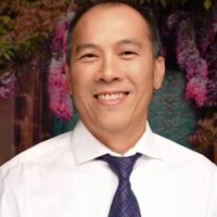
AeroLeads people directory · profile
Timothy Tran Email & Phone Number
Facilities Technical Project and Program Management
at
Applied Materials
1 work email found
@national.com
8 phones found area 408, 510, 585, 207, and 407
LinkedIn matched
✓ Verified July 2026
4 data sources
Profile completeness 100%
Current company
Role
Facilities Technical Project and Program Management
Location
Milpitas, California, United States
Company size
Who is Timothy Tran? Overview
A concise factual answer block for searchers comparing this professional profile.
Quick answer
Timothy Tran is listed as Facilities Technical Project and Program Management at Applied Materials, a with 29658 employees, based in Milpitas, California, United States. AeroLeads shows a work email signal at national.com, phone signal with area code 408, 510, 585, 207, 407, and a matched LinkedIn profile for Timothy Tran.
Timothy Tran previously worked as Facilities Technical Project/Program Management at Applied Materials and Senior Facilities Engineering/Project Manager at Lumileds. Timothy Tran holds Ms, Electrical Engineering from National Technological University.
Company email context
Email format at Applied Materials
This section adds company-level context without repeating Timothy Tran's masked contact details.
{first_initial}{last}@national.com
86% confidence
AeroLeads found 1 current-domain work email signal for Timothy Tran. Compare company email patterns before reaching out.
Profile bio
About Timothy Tran
Over 20 years of experience in developing plasma etch processes for FEOL/BEOL applications in Dielectric and Conductor etch in high-volume manufacturing and equipment companies. More than 3 years of experience in fast-paced R&D environment focusing on solving industry challenges in advanced technology nodes. Experienced in developing Atomic Layer Etch (ALE) processes in both CCP/ICP etchers. Extensive experience in developing applications and supporting a variety of Lam Reliant tools (Lam Rainbow family, Flex family, Kiyo family, and Syndion). Familiar with SiN Atomic Layer Deposition (ALD). Knowledgeable of advanced chip processing techniques, process integration, solid state device physics. Strong skills in problem-solving, hands-on equipment troubleshooting, design of experiment (DOE), statistical process control (SPC). Experienced in working with and managing customers.
Listed skills include Design Of Experiments, Failure Analysis, Semiconductors, Spc, and 7 others.
Current workplace
Timothy Tran's current company
Company context helps verify the profile and gives searchers a useful next step.
Applied Materials
9 roles · 32 years
Timothy Tran work experience
A career timeline built from the work history available for this profile.
Facilities Technical Project/Program Management

Senior Facilities Engineering/Project Manager
• Successfully managed Design-Bid-Build and installed a MOCVD Aixtron reactor including Transfer Module, Abatement systems (Chlorine, Ammonia), Chiller, RF Generator, and other auxiliary support equipment. Obtained required permitting and passed varied city inspections• Perform in-house design and/or manage design-build efforts with external contractors or engineering consultants for tool installation of small to medium sized infrastructure projects• Hold design reviews with external design firms at various stages of the design and permitting process and identify value engineering opportunities. Determine best means of execution for various projects including design-build, or design-bid-build. Work closely with Automation, Environmental, and Safety Engineers on a variety of projects• Track infrastructure capacity including N+1. Support Operations & Maintenance team in troubleshooting and continuous improvement projects related to HVAC, Electrical, Mechanical and Plumbing. Provide budgetary estimates for prospective projects. Develop design scope and submits RFQ to design firms for a variety of facilities projects• Determine most cost-effective method form of bidding for given project including lump sum, GMP, or T&M NTE. Develop scope of work, bid documents, and hold contractor job walks to obtain competitive pricing for a variety of facilities projects including Fab and building architectural, mechanical, electrical, and process piping (MEP) projects• Manage selected contractor’s activities. Ensure adherence to safety standards, code compliance, workmanship, materials selection, adherence to site standard specifications, and quality. Review and respond to submittals and RFI’s• Develop high level project timelines, Gantt charts, etc. to track and insure timely execution of projects. Track budget and spending and inputs into database. Generate purchase requisitions. Perform project punch-list, closeout , as-built documentation, etc.
Feb 2021 - Feb 2023
Senior Facilities Project Manager
Pro Active Business Solutions / Applied Materials
• Managed construction of varied facilities/infrastructure related projects supporting Apps Lab in Buildings 81 & 85 at AMAT.• Successfully completed construction of minor and major facilities infrastructure e.g. Upgraded Solvent Exhaust, FICW system, PCW system; Replaced sanitary sewer line; Installed new equipment in Athena Lab, SFEM FI module, PN2 gas lines etc.• Installed and/or removed semiconductor processing tools in R&D facilities e.g. chamber, FI, pump, chiller, gas lines, etc.• Supported moderate building facilities activities including, but not limited to, expansions, consolidations, and improvements.• Performed detailed coordination of construction: Obtain construction bids from approved suppliers; Develop budget; Obtain permits; Develop appropriate Purchase Requisitions; Coordinate construction activities; Coordinate and attend safety walkthroughs and city inspections; Assist in monitoring vendors for safety compliance, project performance, and schedule performance; Ensure all project schedules meeting customer commitment; Perform all associated pre- and post-project documentation and closure activities; Other responsibilities as assigned by the employer and/or the client.
Feb 2019 - Feb 2021

Senior Staff Process Engineer
- Worked in fast-paced R&D (Advanced Technology Development Group)- Successfully developed novel SCD/ALE PR treatment for EUV patterning to improve LCDU (Local CD Uniformity) to <1.4nm 3σ in both ICP (Kiyo EX) and CCP (Flex GL) tools through Lam/ASML JDP. Applied to TSMC N5 via demo on Flex GL and achieved 1.5nm 3σ LCDU. Co-authored in published paper. - Worked with team to develop low cost multi-patterning (SADP/SAQP) Metal Oxide Spacer on Spacer with PR Mandrel for Memory application on Conductor etcher and transferring to customer site. Collaborated closely with Productivity to develop WAC to meet customer metal contamination specification - Supported Deposition Product Group in Velocity Lab utilizing CPM (Coupon Process Module) to develop SiN ALD in ICP source evaluating 3 different precursors 2nTe (amide), Si2H6, Viper (halide) - Performed demos on varied TSMC N3/N5 applications e.g. SOC, ZrO2, Inpria EUV PR
Sep 2015 - Sep 2018
Staff Field Process Engineer
- Leading etch process engineer responsible for all CIC (Customer Integration Center) projects pertaining to etching (DE: Flex EL/FL, CE: Kiyo EX, TSV: Syndion-C)- Developing QPT process using a-Si Core to provide advanced structures to internal BUs- Successfully developed Spacer based (TiO2) patterning scheme through QPT for 11nm half pitch with <1.5nm 3σ CDU in carbon mask layer. - Enabled EUV lithography with thin resist and improved local CDU. Developed HM and etch processes to deliver <2.5nm local CDU @ 52nm pitch for hole and cut masks with 60-80% shrink from resist to target layer.- Achieved patterning of high AR ≥ 20:1 through DPT in Silicon through use of Oxide HM - Successfully developed a DPT etch process (22nm half pitch) on Silicon target layer with Empire II mask (Granular pattern). Running limited production on a regular basis to supply to internal customers.- Successfully developed an M1 etch process with CNSE Empire-II mask on Flex EL- Provided etch expertise and support to integration projects within CIC and other Product Groups
Feb 2011 - Sep 2014

Cigs Process Engineer
- Responsible for real time process monitoring of all deposition tools (Cu-In-Ga-Se absorber layer), data analysis, improvements to yield, and tool uptime performance- Worked closely with Engineering/Maintenance groups to identify and resolve hardware/software issues; Evaluated new hardware and monitoring controls to drive product/reliability improvements
Jun 2010 - Apr 2011
Sr. Process Engineer
- Customer Technologist Manager (CTM) – Managed UMC etch process technology by actively engaging with customer engineers and local process team to improve existing processes in cost of ownership (COO), yield enhancement, throughput improvement, hardware testing, and collaborated in qualifying new applications- Performed demo projects in R&D lab and at customer sites in both Conductor and Dielectric etch- Supported various international local field accounts to resolve escalations related to hardware, process, failure analysis, and integration issues to gain market share and customer trust- Experienced with Lam Reliant Conductor and Dielectric etch products- Supported global customer base in development and technology transfer by frequent travel
2000 - Jan 2009

Process Engineer
Plasma Etch Process Engineer- Responsible for Oxide etch module overseeing 12 Lam 4520 Oxide etch systems in Class 1 CMOS/BiCMOS Fab- Optimized and monitored critical process parameters utilizing SPC, DOE, FMEA, Lam Station. Set up automation to prevent/eliminate misprocessing. Wrote and trained operators on SOP.- Led a task force of engineering technicians and lead operators in determining root cause of misprocessed lots. Established corrective actions and wrote 8D report closure- Performed cross-functional projects to improve existing products’ cycle time, cost reduction, SPC, yield, equipment utilization- Worked closely with R&D team to develop etch processes for new products- Worked with Integration engineers to improve parametric yield, final yield, reliability etc.- Sustained Poly & Nitride etch applications on Lam 4420 etchers and Photolithography module
1995 - 2000
~5 yrs
Team & coworkers
Colleagues at Applied Materials
Other employees you can reach at appliedmaterials.com. View company contacts for 29658 employees →
HH
 Htay Hlaing
Colleague at Applied MaterialsSunnyvale, California, United States
View →
AA
Htay Hlaing
Colleague at Applied MaterialsSunnyvale, California, United States
View →
AA
 Aryabrata Acharya
Colleague at Applied MaterialsBengaluru, Karnataka, India
View →
AE
Aryabrata Acharya
Colleague at Applied MaterialsBengaluru, Karnataka, India
View →
AE
 Armando Ellana
Colleague at Applied MaterialsSingapore
View →
TR
Armando Ellana
Colleague at Applied MaterialsSingapore
View →
TR
 Tarun Raheja
Colleague at Applied MaterialsBengaluru, Karnataka, India
View →
GJ
Tarun Raheja
Colleague at Applied MaterialsBengaluru, Karnataka, India
View →
GJ
 Glenn Jules
Colleague at Applied MaterialsDel Valle, Texas, United States
View →
AJ
Glenn Jules
Colleague at Applied MaterialsDel Valle, Texas, United States
View →
AJ
 Anthony Jay Aratia
Colleague at Applied MaterialsPhilippines
View →
KA
Anthony Jay Aratia
Colleague at Applied MaterialsPhilippines
View →
KA
 Kenneth Ainslie
Colleague at Applied MaterialsDublin, California, United States
View →
WY
Kenneth Ainslie
Colleague at Applied MaterialsDublin, California, United States
View →
WY
 Wai-Fan Yau
Colleague at Applied MaterialsSan Jose, California, United States
View →
RR
Wai-Fan Yau
Colleague at Applied MaterialsSan Jose, California, United States
View →
RR
 Ranjani Ravindrabharathy
Colleague at Applied MaterialsSan Francisco Bay Area, United States
View →
AT
Ranjani Ravindrabharathy
Colleague at Applied MaterialsSan Francisco Bay Area, United States
View →
AT
 Andrew Torres
Colleague at Applied MaterialsWarsaw, Mazowieckie, Poland
View →
Andrew Torres
Colleague at Applied MaterialsWarsaw, Mazowieckie, Poland
View →
Htay Hlaing
Colleague at Applied MaterialsSunnyvale, California, United States
View →
AA
Aryabrata Acharya
Colleague at Applied MaterialsBengaluru, Karnataka, India
View →
AE
Armando Ellana
Colleague at Applied MaterialsSingapore
View →
TR
Tarun Raheja
Colleague at Applied MaterialsBengaluru, Karnataka, India
View →
GJ
Glenn Jules
Colleague at Applied MaterialsDel Valle, Texas, United States
View →
AJ
Anthony Jay Aratia
Colleague at Applied MaterialsPhilippines
View →
KA
Kenneth Ainslie
Colleague at Applied MaterialsDublin, California, United States
View →
WY
Wai-Fan Yau
Colleague at Applied MaterialsSan Jose, California, United States
View →
RR
Ranjani Ravindrabharathy
Colleague at Applied MaterialsSan Francisco Bay Area, United States
View →
AT
Andrew Torres
Colleague at Applied MaterialsWarsaw, Mazowieckie, Poland
View →
2 education records
Timothy Tran education
Ms, Electrical Engineering
National Technological University
Bs, Microelectronics Engineering
Rochester Institute Of Technology
FAQ
Frequently asked questions about Timothy Tran
Quick answers generated from the profile data available on this page.
What company does Timothy Tran work for?
Timothy Tran works for Applied Materials.
What is Timothy Tran's role at Applied Materials?
Timothy Tran is listed as Facilities Technical Project and Program Management at Applied Materials.
What is Timothy Tran's email address?
AeroLeads has found 1 work email signal at @national.com for Timothy Tran at Applied Materials.
What is Timothy Tran's phone number?
AeroLeads has found 8 phone signal(s) with area code 408, 510, 585, 207, 407 for Timothy Tran at Applied Materials.
Where is Timothy Tran based?
Timothy Tran is based in Milpitas, California, United States while working with Applied Materials.
What companies has Timothy Tran worked for?
Timothy Tran has worked for Applied Materials, Lumileds, Pro Active Business Solutions / Applied Materials, Lam Research, and Solyndra.
Who are Timothy Tran's colleagues at Applied Materials?
Timothy Tran's colleagues at Applied Materials include Htay Hlaing, Aryabrata Acharya, Armando Ellana, Tarun Raheja, and Glenn Jules.
How can I contact Timothy Tran?
You can use AeroLeads to view verified contact signals for Timothy Tran at Applied Materials, including work email, phone, and LinkedIn data when available.
What schools did Timothy Tran attend?
Timothy Tran holds Ms, Electrical Engineering from National Technological University.
What skills is Timothy Tran known for?
Timothy Tran is listed with skills including Design Of Experiments, Failure Analysis, Semiconductors, Spc, Etching, Metrology, Semiconductor Industry, and Characterization.
Find 750M verified contacts
Search by job title, company, industry, location, and seniority. Export verified B2B contact data when you need it.
Start free trial