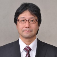
Specialist And Air-Con Systems Lab And Home Appliance Laboratory R And D Center
Hisense Japan
Please complete the CAPTCHA to continue
@littelfuse.com
✓
LinkedIn matched
A concise factual answer block for searchers comparing this professional profile.
Takeshi Kuwahara is listed as Specialist and Air-con Systems Lab and Home Appliance Laboratory R and D Center at Hisense Japan, based in Tokyo, Japan. AeroLeads shows a work email signal at littelfuse.com and a matched LinkedIn profile for Takeshi Kuwahara.
Takeshi Kuwahara previously worked as Specialist / Air-con Systems Lab / Home Appliance Laboratory R&D Center at Hisense Japan and Sr. Engineer II, Field Application at Littelfuse. Takeshi Kuwahara holds 学士, Electrical And Electronics Engineering from 神奈川大学 / Kanagawa University.
This section adds company-level context without repeating Takeshi Kuwahara's masked contact details.
AeroLeads found 1 current-domain work email signal for Takeshi Kuwahara. Compare company email patterns before reaching out.
Specialist of electric circuit design1) Analog & Digital circuit designInverter circuit, Motor driving, Plasma display sustain circuit, Power supply circuit, Graphic circuit, Circuit simulation on P-SIM2) LSI and FPGA designVHDL, Verilog-HDL, Circuit simulation, Altera3) ProgrammingC, Visual Basic, Assembler ,MPU programming4) Product designEMI noise reduction, Quality estimation, Test method, Mass-production document drawing5) SupportCuster design support, Trouble shooting, Product start-up in oversea factory6) Computer skillFilemaker database design, Web site design, EXCEL VBA
Listed skills include Electrical Engineering, Analog Circuit Design, Product Design, Digital Circuit Design, and 2 others.
Company context helps verify the profile and gives searchers a useful next step.
A career timeline built from the work history available for this profile.
Tokyo, Jp
日本 神奈川県 川崎市

日本 東京
Support IXYS’s power semiconductor products for Japan and Korea market

日本 東京都 23 区内
Tokyo SEC (Solution Engineering Center)- Support for motor drive solution Hardware and software development Motor measurement system Motor driving algorithm analysis- Applicaton support BLDC(Brushless DC), BDC(Brushed DC) and Stepping Motor HVAC, EOP, EWP, FAN motor, Compressor (Home appliance, Automotive and Industrial area)- Power translation circuit Inverter, DC-AC, DC-DC.- PCB design Analog and digital mixed circuit- Software design Visual Studio C#, Arduino IDE- Circuit simulation P-SIM
日本 神奈川県 横浜市
Technology venture in power conversion and motor driving area.Hardware engineering - Motor driving, Power electronics » Developed inverter for electric motor assisted bicycle- Leading the development team for Bicycle product (Co-working with Nidec)- Developed discrete inverter circuit design and STM32 32-bit microcontrollers based MPU program. » Developed Myway pCUBE* (500V version) * pCUBE : 10 kW-class regenerative type direct current power supply- Hardware design, debug, product test for launching 500 voltage new version - Coordinated product test of whole unit and circuit level. (A/D adjustment for high precision), Test program- Participated production transfer with new partner Technical support, Improved yield rate, Documentation, Failure analysis- Motor test bench System design, Testing and Documentation

日本 東京都
Hardware engineering – Inverter, Motor driving, Plasma display » Home appliance inverter circuit design (2009-2012) - Developed inverter circuit for compressor driving. (4kW-class Air-conditioner outdoor unit, Refrigerator) - Developed 1-shunt sensor-less motor driving, bridge-less PFC Feasibility test of high efficiency and low cost circuit topology. - Developed IPM (INV+PFC, Super-Junction MOSFET) (Co-working with Mitsubishi, Sanyo, Rohm)- Researched SiC MOSFET and SBD for feasibility. (Co-working with Rohm)- Technical supporting for AC laboratory in ChangWong, Korea» Plasma display circuit design (2004-2008)- Initiate launching 2nd and 3rd PDP factory in Gumi, Korea. Failure-analysis investigation- Developed semi-customed semiconductor for PDP drive circuit. Hi-voltage Data and scan drive IC ,IPM, IGBT and HVIC (Co-working with Renesas, Fuji Electronics, Toshiba, Rohm, Panasonic)- Participated taks team for improving yield rate, cost ,quality issues and performance. (Co-working with Fuji electronics , Sanyo semiconductor, STMicro, Shindo, LG Inotech)- Lead development team for PDP in Japan Manage job between R&D in Korea and co-workers in Japan Direct report to R&D executive in Korea HQ- Technical supporting for Display laboratory in Seoul, Korea.

日本 神奈川県 川崎市
Hardware engineering – Plasma display» Plasma display driving circuit design (1996-2004) - Lead development team of 32 inch to 42 inch PDP series. - Participate circuit design, product quality test, customer support, plant support, documentation- Certificated Product Safety standard (IEC 60950/UL 60950) and Test - Open-short circuit test, AC Line noise, ESD test, Creation of the documents for a safety standard application, measured and improved electro-magnetic emission noise and mulfunction, Failure-analysis investigation- Developed IPM (Intelligent Power Module), HVIC (Hi-Voltage Integrate Circuit) and Gate coupler for discreat design PDP drive circuit. - Contributed mass product of ALiS(*1) driving method for world-fast High Definition PDP. Developed high voltage and high speed switching circuit design for sustainer circuit. (*1) 1st HD Plasma Display in the world- Developed LSI for display data conversion circuit- Customer support Solved various issues of using PDP module in TV unit. (EMI,Interface,Power supply) (TV supplier : Sony, Hitachi, Sanyo, Philips, Fujitsu-General) - Participated launching PDP module factory #2 in Miyazaki, Japan. Trouble shooting, Improve yield rate, Fault analysis

Hardware engineering – PC» Notebook PC design for North America market, ASIC design (1989-1996) - Developed PC circuit and estimated whole product Design UltraLite series :Intel 86 based Notebook PC. Perform mother board design- graphic controller for STN-LCD panel FPGA (Altera, Xilinx) and ASIC design, VHDL entry, - Supported technical issue PC assembly factory in Boston, U.S.A To improve failure rate in the market, failure analysis, repair program- Certificated Product Safty standard (UL 950) and test Creation of the documents for a safety standard application, Line noise, ESD test, EMI, power on/off sequence, power source break test

Quick answers generated from the profile data available on this page.
Takeshi Kuwahara works for Hisense Japan.
Takeshi Kuwahara is listed as Specialist and Air-con Systems Lab and Home Appliance Laboratory R and D Center at Hisense Japan.
AeroLeads has found 1 work email signal at @littelfuse.com for Takeshi Kuwahara at Hisense Japan.
Takeshi Kuwahara is based in Tokyo, Japan while working with Hisense Japan.
Takeshi Kuwahara has worked for Hisense Japan, Littelfuse, On Semiconductor, Myway Plus Corporation, and Lg Electronics.
You can use AeroLeads to view verified contact signals for Takeshi Kuwahara at Hisense Japan, including work email, phone, and LinkedIn data when available.
Takeshi Kuwahara holds 学士, Electrical And Electronics Engineering from 神奈川大学 / Kanagawa University.
Takeshi Kuwahara is listed with skills including Electrical Engineering, Analog Circuit Design, Product Design, Digital Circuit Design, High Voltage, and Motor Drives.
Search by job title, company, industry, location, and seniority. Export verified B2B contact data when you need it.
Start free trial Search contactsCheck these profiles if this is not the Takeshi Kuwahara you were looking for.