기계 엔지니어
Current
Jul 2022 - Present
Please complete the CAPTCHA to continue
A concise factual answer block for searchers comparing this professional profile.
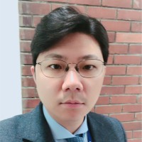
김상균 is listed as data analyst | semiconductor engineering | RPA Engineering | quality engineer | R&D at Samsung Electronics, a with 118428 employees, based in Hwaseong, Gyeonggi, Korea, Republic of. AeroLeads shows a matched LinkedIn profile for 김상균.
김상균 previously worked as 기계 엔지니어 at Samsung Electronics and 엔지니어 at Sk실트론. 김상균 holds 학사, 응용화학공학 from 경북대학교(Kyungpook National University).
This section adds company-level context without repeating 김상균's masked contact details.
Review company-level records connected to 김상균 before choosing the right outreach path.
1. 프로젝트 명 : 200mm SEC PMIC (S3) Edge Defocus 개선-.프로젝트 기간 및 인원 : 2020.03~2021.03 (12개월), 3명-.프로젝트 성과 : PMIC(S3) Edge Profile(Alpha Step) 최적화-. My Role : Edge 0.5mm 영역 고객 수율 향상을 위한 Polishing Chemical 개발 및 양산 조건 확보-. 획득 역량 : Polishing Slurry의 이해 및 Edge Profile 개선을 위한 Polishing Recipe 개발 역량 획득2. 프로젝트 명 : 200mm SEC DDI Cone Defect 개선-. 프로젝트 기간 및 인원 : 2020.05~2020.07 (3개월), 3명-. 프로젝트 성과 : STI 공정 이후 측정단 Flat Zone 부위 확산형 Cone Defect 원인 규명 및 개선-. My Role : 장비 재현성 평가를 통한 원인 규명 및 장비 강건화 (Contact 부위 최소화)-. 역량 : XRT, OP-MCTL 분석 역량 획득. Edge 부위 이상 발생시 고객 수율 영향성에 대한 이해.3. 프로젝트 명 : Polishing 공정 LLS (Wafer 표면 결함) 개선-. 프로젝트 기간 및 인원 : 2019.12~2020.03 (4개월), 2명-. 프로젝트 성과 : Final Polishing 공정 온도/압력 최적화를 통한 Wafer Pit Defect 영구 개선-. My Role : Data Mining (Minitab Tool 사용) 및 장비 Test 업무 수행-. 획득 역량 : Single Wafer Polishing 공정의 온도/압력 상관 관계 이해, Data Mining 역량 획득3. 프로젝트 명 : Spotfire개발을 통한 수율 분석 System 구축-. 프로젝트 기간 및 인원 : 2019.02~2019.08 (7개월), 2명-. 프로젝트 성과 : FTY, RTY 분석 Tool 개발 (Spotfire 사용)-. My Role : 전산, 실물 일치화 및 작업 방법 최적화-. 획득 역량 : FTY, RTY 분석역량 획득, 수율 개선 Point Finding 역량 획득
Company context helps verify the profile and gives searchers a useful next step.
A career timeline built from the work history available for this profile.
대한민국 구미
Other employees you can reach at samsung.com. View company contacts for 118428 employees →
 Michael (Myunghwa) Shin
Colleague at Samsung ElectronicsSeoul Incheon Metropolitan Area, Korea, Republic Of
View →
SB
Michael (Myunghwa) Shin
Colleague at Samsung ElectronicsSeoul Incheon Metropolitan Area, Korea, Republic Of
View →
SB
 Siddharth Bathla
Colleague at Samsung ElectronicsGurgaon, Haryana, India
View →
SK
Siddharth Bathla
Colleague at Samsung ElectronicsGurgaon, Haryana, India
View →
SK
 Seji Kim
Colleague at Samsung ElectronicsSeoul Incheon Metropolitan Area, Korea, Republic Of
View →
AK
Seji Kim
Colleague at Samsung ElectronicsSeoul Incheon Metropolitan Area, Korea, Republic Of
View →
AK
 Amit Kumar
Colleague at Samsung ElectronicsChorasi, Gujarat, India
View →
PA
Amit Kumar
Colleague at Samsung ElectronicsChorasi, Gujarat, India
View →
PA
 Paulo Augusto
Colleague at Samsung ElectronicsCampinas, São Paulo, Brazil
View →
AS
Paulo Augusto
Colleague at Samsung ElectronicsCampinas, São Paulo, Brazil
View →
AS
 Avhi Singh
Colleague at Samsung ElectronicsKakori, Uttar Pradesh, India
View →
ZE
Avhi Singh
Colleague at Samsung ElectronicsKakori, Uttar Pradesh, India
View →
ZE
 Zakeria Elsayed
Colleague at Samsung ElectronicsEgypt
View →
DH
Zakeria Elsayed
Colleague at Samsung ElectronicsEgypt
View →
DH
 Duong Hue
Colleague at Samsung ElectronicsVietnam, Viet Nam
View →
SP
Duong Hue
Colleague at Samsung ElectronicsVietnam, Viet Nam
View →
SP
 Sebastian Partsch
Colleague at Samsung ElectronicsMiami, Florida, United States
View →
JC
Sebastian Partsch
Colleague at Samsung ElectronicsMiami, Florida, United States
View →
JC
 Jinwoo Choi
Colleague at Samsung ElectronicsSouth Korea, Korea, Republic Of
View →
Jinwoo Choi
Colleague at Samsung ElectronicsSouth Korea, Korea, Republic Of
View →

Activities and Societies: 교내 방송국 (엔지니어), 도서관 학생위원회 (시설팀장), 학과 학생회 (인사팀장) 1. 신규제품 수율 안정성에 이바지하는 Product Engineer 저는 출하 전 최종 품질과 가장 가까운.
Quick answers generated from the profile data available on this page.
김상균 works for Samsung Electronics.
김상균 is listed as data analyst | semiconductor engineering | RPA Engineering | quality engineer | R&D at Samsung Electronics.
김상균 is based in Hwaseong, Gyeonggi, Korea, Republic of while working with Samsung Electronics.
김상균 has worked for Samsung Electronics, Sk실트론, and Sk Siltron Css.
김상균's colleagues at Samsung Electronics include Michael (Myunghwa) Shin, Siddharth Bathla, Seji Kim, Amit Kumar, and Paulo Augusto.
You can use AeroLeads to view verified contact signals for 김상균 at Samsung Electronics, including work email, phone, and LinkedIn data when available.
김상균 holds 학사, 응용화학공학 from 경북대학교(Kyungpook National University).
Search by job title, company, industry, location, and seniority. Export verified B2B contact data when you need it.
Start free trial Search contactsCheck these profiles if this is not the 김상균 you were looking for.