
Verified email-pattern data for Holistep is currently limited. You can still use the company insights and contact sections below.
To achieve ever shrinking dimensions and higher resolutions of circuit elements, projection lithography (PL), is growing in complexity and cost to manufacturers. It is limited to producing 2D images on flat surfaces. Extension to 3D imaging is restricted by trade-off between focus depth and resolution. Advanced, cost-efficient solutions to fabricate wafer-scale 3D components are required.
HoLiSTEP unleashes the potential of sub-wavelength Holographic Lithography (HL) as a powerful and enabling disruptive lithography. HL will overcome limitations of PL and facilitate production of novel 3D topographies with high resolution while making the production of high resolution IC much more affordable.
Company Details
- Employees
- 1
- Address
- Dresden
- Industry
- Research Services
- Website
- http://holistep.org
Holistep Questions
HoLiSTEP's website is http://holistep.org
HoLiSTEP's LinkedIn profile is https://www.linkedin.com/company/holistep-project
HoLiSTEP has
1 employees.
View email and phone details for 1
employees at HoLiSTEP.
HoLiSTEP's industry is
Research Services
HoLiSTEP's top competitors are
Holistep,
Fhf Bretagne,
Modus Research And Innovation,
Innolas Photonics Gmbh,
Swhl Gmbh,
Politrempe Sa,
River Severn Partnership Advanced Wireless Innovation Region,
Vistec,
Fraunhofer Enas,
Générale Ressorts Sa.
HoLiSTEP's categories are Research Services
Explore related pages
Related company profiles:


Top HoLiSTEP Employees
-

Danny Reuter
Head Of Department Nano Device…
Greater Chemnitz Area, Germany1enas.fraunhofer.de
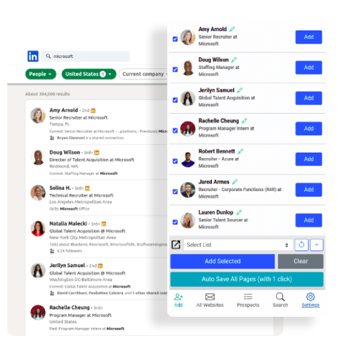
Free Chrome Extension
Find emails, phones & company data instantly
Find verified emails from LinkedIn profiles
Get direct phone numbers & mobile contacts
Access company data & employee information
Works directly on LinkedIn - no copy/paste needed
Aero Online
Your AI prospecting assistant
Select data to include:
Total price:
$0.00
0 records × $0.02 per record
How It Works
Get a Free Account
Sign up for a free account. No credit card required. Up to 10 free credits.

Search the #1 Contact Database
Get contact details of over 750M+ profiles across 60M companies – all with industry-leading accuracy. Sales Navigator and Recruiter users, try out our Email Finder Extension.
Use our AI-Powered Email Finder
Find business and personal emails and mobile phone numbers with exclusive coverage across niche job titles, industries, and more for unparalleled targeting. Also available via our Contact Data API.