
Principal Physical Design Engineer
Current
Sep 2021 - Present
Please complete the CAPTCHA to continue
@maxlinear.com
✓
LinkedIn matched
A concise factual answer block for searchers comparing this professional profile.
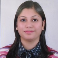
Alka Garg is listed as Principal physical design engineer at MaxLinear, a with 889 employees, based in Singapore. AeroLeads shows a work email signal at maxlinear.com and a matched LinkedIn profile for Alka Garg.
Alka Garg previously worked as Senior Staff physical design Engineer at Realtek Semiconductor Corp. and Senior Physical Design Engineer at Intel Corporation. Alka Garg holds Btech, Computer Engineering from Aligarh Muslim University.
This section adds company-level context without repeating Alka Garg's masked contact details.
AeroLeads found 1 current-domain work email signal for Alka Garg. Compare company email patterns before reaching out.
Alka Garg is a Principal physical design engineer at MaxLinear. She possess expertise in functional verification, soc. Colleagues describe her as " “A great honor to work with” is the phrase that comes to mind when I think about Alka. I’ve had the pleasure of knowing Alka for 7 years, during which I was her manager at ST Ericsson and Intel collaborating on many wireless and GNSS projects. Above all, I was impressed with Alka’s ability to listen and learn new skills. Initially from a verification program management role, she challenged herself to come back to a more technical role. She became the go-to person for IRDROP analysis, on top of covering over the years most of topics of RTL2GDS activity. She was also the successful lead of the GNSS macro that will be shipping soon in millions of IPhone 11. Alka would be a true asset for any positions requiring a wide scope of RTL2GDS skills and comes with my heartfelt recommendation. " and "I have worked with Alka for 6 months for the re-design of an IP block where Alka was responsible from all the verification tasks of that IP block and I was the IP project leader. I worked with her remotely. She is an organized person, listens well and implements well. Always respectful and kind to the people. It was very efficient and easy to work with her remotely. During the project, she has proven her technical skills in IC verification many times. I really appreciated the work she has done and would love to work with her again."
Listed skills include Functional Verification and Soc.
Company context helps verify the profile and gives searchers a useful next step.
A career timeline built from the work history available for this profile.


Singapore
GNSS IP Project: GNSS IP to be used for 5G modem subsystem for mobile application. Project is completed in various technologies, Intel C14, TSMC C16, TSMC C28HPC+Principal Responsibility:• Technical Lead for the GNSS project in C28HPC+ tech. I was responsible for complete flow from synthesis to tapeout. Apart from managing schedule and looking after KPI to meet for power reduction. My responsibilities include synthesis, UPF, LEC, Power management, STA, and Irdrop analysis. Worked with Back-end engineer to provide constant feedback for clock enhancement, power recovery and ECO implementation.• IRdrop analysis for GNSS IP in C16/C14/C28 technology. Connectivity Projects: WIFI Bluetooth Combo subsystem designed for Intel PC group in C28 technology.Principal Responsibilities:• Power and Irdrop Analysis: Did various analysis like static, rampup, dynamic to check robustness of power grid. Performed power analysis using vectors, detailed analysis of results to see if power can be improved.o STA for DFT modes: Worked with DFT and architecture team and created constraints for various DFT modes(Bist/stuckat/scan/atspeed). Completed STA run and analysis for DFT modes.

Singapore
Project: Development of a connectivity chip with ultra-low power consumption, comprising of NFC, GPS/GLONASS, BT, and FM controller targeting smart phones and tablets market. Device is targeted in 40nm technology.Achievement: • Risk management–Identified risks, uncertainties and potential problems which could affect project execution. Handled risk assessment and took appropriate action to solve them.• Worked with cross functional team and created and executed detailed SoC level bottom-up schedule to follow STEPP (ST-Ericsson Product Process).• Ensured that deliverables are on time .Worked with IP organization and SOC team leads and acted proactively to avoid any delay on the schedule. • Worked with IP organization and ensured IP quality is good to achieve first pass success.• Managed SoC CCB(change control board). • Coached the team on ST Ericsson product development cycle and quality control processes.
Singapore
Design Verification Lead (June’09-Aug’11)Achievement: • Built a new team for design verification activities of Bluetooth subsystem for two products. Transferred design verification activities from France to Singapore and executed DV tasks with quality and on-time. Also managed third party contractor to deliver work with quality and on-schedule.• Managed resources and team performance appraisals for very complex products which are running in parallel and to be completed with-in very short span of time.Project: Bluetooth IP subsystem Verification Lead Achievement:• Grew a team to 13 members and brought to full potential and productive within short span of time.• Achieved IP delivery on time to meet project schedule and customer requirement.• Demonstrated strong leadership by managing cross geographical functional teams.• Vendor management- managed Einfochip to deliver project to meet quality requirement and to meet schedule.• Led and drove team for excellence by improving quality of verification by introducing random verification (SV-OVM) methodology, which resulted in finding many bugs in existing verified RTL.• Managed team to fix over 200 PR-CR with-in very short period of time.• Achieved 98% code coverage and 100% functional coverage.• Created SV-OVM VIP and achieved 100% code and functional coverage for module SPIE.• Worked with SOC team and achieved successful IP integration for the complex SOC project.Project: Castor IP (NFC subsystem) Project ManagerAchievement:• Built a new team for NFC IP development. Coached the FE design and design verification leads regularly.• Proactively took ownership to revive project schedule and to bring project to closure.• Managed resources and handled their performance appraisal.• Managed and coordinated geographical team to meet project schedule.• Cultivated good relationship and motivated team to drive for excellence.

Singapore
Project: Design and implementation of USB 3.0 slave controller which includes a new, higher speed bus called SuperSpeed , which supports speed upto 5Ghz.Achievement: Successfully verified Protocol layer for USB3IP.• Developed BFM, Monitor, Scoreboard, and test environment in e-language for Protocol layer verification.• Achieved 100% functional coverage for priority1 and priority 2 features for protocol layer.• Created automated sequence lib with capability of all random out transaction with all types of error injection.• Co-ordinate with different module RTL designer for IP integration testing. Successfully made one OUT transaction pass with all USB3 layers integrated.
Singapore
Senior IC Design Engineer (July'03 – Dec’07) Project: Design and implementation of Wireless USB device which enables USB peripherals to communicate with Host without using USB cables. This project is done in collaboration with Philips semiconductor Eindhoven and Singapore. Achievement: • Created design verification environment and wrote tests using SPECMAN and E-language to verify WiFi MBOA MAC beacon processing. Performed equivalence checking on completed MBOA MAC controller. Also integrated and tested memory bists at top level.Project: ULPI (UTMI+ Low Pin Count Interface) transceiver, ULPI allows chip and system designers to connect a Hi-Speed USB transceiver to USB core logic embedded in ASICs and systems-on-chip (SoCs).Achievement:• Being an IC lead for the Project , worked with the team members to solve different issues for backend, analog, FPGA and Silicon testing • Providing customers encrypted model and responding to them on there queries and helping them to solve issue with integration and bugs.• Actively involved in development of ULPI Specification 1.0• Top level integration of design, verification and Synthesis of ULPI transceiver and ULPI Link wrapper.• DFT Insertion, generation and verification of functional test vectors using Philips in-house tools.• Worked on Formal verification, Clock tree synthesis and STA, Timing Closure to meet the specifications.
Gurgaon, India
Achievement: Design, synthesis and verification of Motorola’s SoC Designs (System on Chip) used for motor control and wireless communication. Project: DBMX1+ is part of Motorola’s Dragonball™ family and is ARM9 based 3G embedded applications processor used for PDA & smart phones, developed in 0.13u technology.Achievement:• Verified USBOTG (Universal Serial Bus- On the Go) core at chip/system level and from application perspective.• Set up the environment using C and verilog HDL for system level verification and gave training to the team for using the environment.Project: Worked on 5 DSP controllers which are part of Motorola HawkV1 and HawkV2 DSP processor family and used for general purpose application processor developed in 0.25u and 0.18u technology.Achievement:• RTL design, synthesis and verification of TOD (Time of Day) module • System/chip level verification of various chip modules like MPIO, SCI(Serial communication interface), SPI(Serial Peripheral Interface), GPIO(General Purpose Input Output), EXBIU(External bus interface), ITCN(Interrupt controller), SIM(System Integration module), CLKGEN(Clock generation module), COP(Computer operating properly module), PWM (Pulse Width Modulator), FIU( Flash Interface Unit) and low power modes. Verification is done using tartan flow, environment is developed using C/ASM/Verilog/ shell script.• Developed the flow for chip level formal verification of Monza using Verplex LEC and Synopsys Formality. Bench marked both tools for the project.• Generated vectors for IDD, ESD/Latch-up and AC test characterization of chip after Silicon• Architecture design (Spec development), RTL coding and synthesis of TMUX, TLM (Tap linking module, which select CORE JTAG and CHIP JTAG depending upon some test registers and test modes.
Other employees you can reach at maxlinear.com. View company contacts for 889 employees →
 Antonio Arregui
Colleague at MaxlinearGreater Valencia Metropolitan Area, Spain
View →
LM
Antonio Arregui
Colleague at MaxlinearGreater Valencia Metropolitan Area, Spain
View →
LM
 Lorenzo Marchionini
Colleague at MaxlinearMunich, Bavaria, Germany
View →
NA
Lorenzo Marchionini
Colleague at MaxlinearMunich, Bavaria, Germany
View →
NA
 Nikitha Aravapalli
Colleague at MaxlinearBengaluru, Karnataka, India
View →
SK
Nikitha Aravapalli
Colleague at MaxlinearBengaluru, Karnataka, India
View →
SK
 Shanavas Kottikal
Colleague at MaxlinearBengaluru, Karnataka, India
View →
MW
Shanavas Kottikal
Colleague at MaxlinearBengaluru, Karnataka, India
View →
MW
 Max Wu
Colleague at MaxlinearTaipei City, Taiwan, Province Of China
View →
BS
Max Wu
Colleague at MaxlinearTaipei City, Taiwan, Province Of China
View →
BS
 Begoña Sanchez Esquibel
Colleague at MaxlinearGreater Valencia Metropolitan Area, Spain
View →
BG
Begoña Sanchez Esquibel
Colleague at MaxlinearGreater Valencia Metropolitan Area, Spain
View →
BG
 Balaji Gnanasekaran
Colleague at MaxlinearGreater Chennai Area, India
View →
A(
Balaji Gnanasekaran
Colleague at MaxlinearGreater Chennai Area, India
View →
A(
 Anderson (Pinyang) Wang
Colleague at MaxlinearHsinchu City, Taiwan, Province Of China
View →
AB
Anderson (Pinyang) Wang
Colleague at MaxlinearHsinchu City, Taiwan, Province Of China
View →
AB
 Abhilash B
Colleague at MaxlinearBengaluru East, Karnataka, India
View →
MC
Abhilash B
Colleague at MaxlinearBengaluru East, Karnataka, India
View →
MC
 M Cai
Colleague at MaxlinearShenzhen, Guangdong, China
View →
M Cai
Colleague at MaxlinearShenzhen, Guangdong, China
View →

Quick answers generated from the profile data available on this page.
Alka Garg works for MaxLinear.
Alka Garg is listed as Principal physical design engineer at MaxLinear.
AeroLeads has found 1 work email signal at @maxlinear.com for Alka Garg at MaxLinear.
Alka Garg is based in Singapore while working with MaxLinear.
Alka Garg has worked for Maxlinear, Realtek Semiconductor Corp., Intel Corporation, St-Ericsson, and Nxp.
Alka Garg's colleagues at MaxLinear include Antonio Arregui, Lorenzo Marchionini, Nikitha Aravapalli, Shanavas Kottikal, and Max Wu.
You can use AeroLeads to view verified contact signals for Alka Garg at MaxLinear, including work email, phone, and LinkedIn data when available.
Alka Garg holds Btech, Computer Engineering from Aligarh Muslim University.
Alka Garg is listed with skills including Functional Verification and Soc.
Search by job title, company, industry, location, and seniority. Export verified B2B contact data when you need it.
Start free trial Search contactsCheck these profiles if this is not the Alka Garg you were looking for.
View similar profiles